Fast and Highly Sensitive Ionic Polymer Gated WS$_2$-Graphene Photodetectors
Jake D. Mehew, Selim Unal, Elias Torres Alonso, Gareth F. Jones, Saad, Fadhil Ramadhan, Monica F. Craciun, and Saverio Russo

TL;DR
This paper introduces ionic polymer gated WS₂-graphene heterostructure photodetectors that achieve high sensitivity and operate at bandwidths up to 1.5 kHz, suitable for real-time imaging, by effectively screening charge traps and tuning the Fermi level.
Contribution
The study demonstrates a novel ionic polymer encapsulation technique enabling fast, highly sensitive graphene-WS₂ photodetectors with unprecedented bandwidth and responsivity.
Findings
Bandwidth up to 1.5 kHz achieved
Responsivity of 10^6 A/W demonstrated
Detectivity of 3.8×10^11 Jones reported
Abstract
The combination of graphene with semiconductor materials in heterostructure photodetectors, has enabled amplified detection of femtowatt light signals using micron-scale electronic devices. Presently, the speed of such detectors is limited by long-lived charge traps and impractical strategies, e.g. the use of large gate voltage pulses, have been employed to achieve bandwidths suitable for applications, such as video-frame-rate imaging. Here, we report atomically thin graphene-WS heterostructure photodetectors encapsulated in an ionic polymer, which are uniquely able to operate at bandwidths up to 1.5 kHz, whilst maintaining internal gain as large as . Highly mobile ions and a nanometre scale Debye length of the ionic polymer are used to screen charge traps and tune the Fermi level of graphene over an unprecedented range at the interface with WS. We observe a responsivity…
Click any figure to enlarge with its caption.
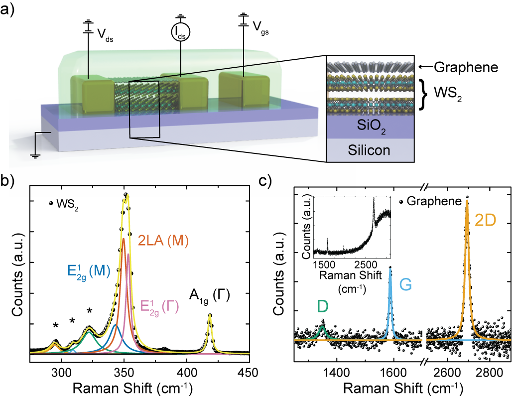 Figure 1
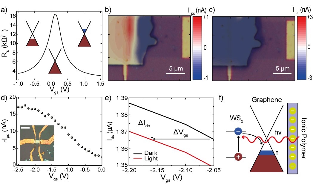 Figure 2
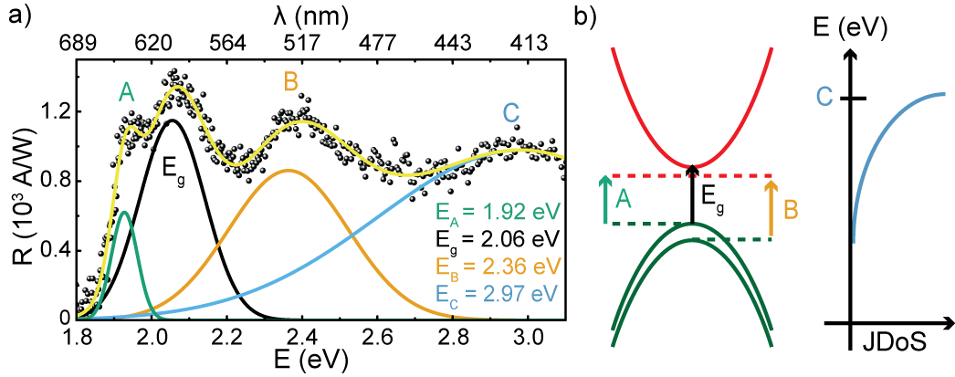 Figure 3
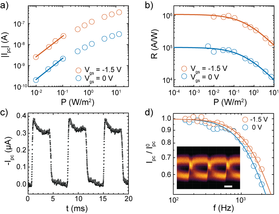 Figure 4
Peer Reviews
No public reviews on file for this paper yet. If you reviewed it on a platform where reviews are public (OpenReview, ICLR, NeurIPS, ICML), you can paste yours below so the community can read it here.
Videos
No videos yet. Explain this paper in a talk, walkthrough, or lecture? Add one.
Fast and Highly Sensitive Ionic Polymer Gated \ceWS2-Graphene Photodetectors
Jake D. Mehew
Centre for Graphene Science, College of Engineering, Mathematics and Physical Sciences, University of Exeter, Exeter, EX4 4QL, UK
EPSRC Centre for Doctoral Training in Metamaterials, College of Engineering, Mathematics and Physical Sciences, University of Exeter, Exeter, EX4 4QL, UK
Both authors contributed equally to this work
Selim Unal
Centre for Graphene Science, College of Engineering, Mathematics and Physical Sciences, University of Exeter, Exeter, EX4 4QL, UK
Both authors contributed equally to this work
Elias Torres Alonso
Centre for Graphene Science, College of Engineering, Mathematics and Physical Sciences, University of Exeter, Exeter, EX4 4QL, UK
Gareth F. Jones
Centre for Graphene Science, College of Engineering, Mathematics and Physical Sciences, University of Exeter, Exeter, EX4 4QL, UK
Saad Fadhil Ramadhan
Centre for Graphene Science, College of Engineering, Mathematics and Physical Sciences, University of Exeter, Exeter, EX4 4QL, UK
Department of Physics, College of Science, University of Duhok, Duhok, 42001 Kurdistan Region, Iraq
Monica F. Craciun
Centre for Graphene Science, College of Engineering, Mathematics and Physical Sciences, University of Exeter, Exeter, EX4 4QL, UK
Saverio Russo
Centre for Graphene Science, College of Engineering, Mathematics and Physical Sciences, University of Exeter, Exeter, EX4 4QL, UK
Email: [email protected]
Abstract
The combination of graphene with semiconductor materials in heterostructure photodetectors, has enabled amplified detection of femtowatt light signals using micron-scale electronic devices. Presently, the speed of such detectors is limited by long-lived charge traps and impractical strategies, e.g. the use of large gate voltage pulses, have been employed to achieve bandwidths suitable for applications, such as video-frame-rate imaging. Here, we report atomically thin graphene-\ceWS2 heterostructure photodetectors encapsulated in an ionic polymer, which are uniquely able to operate at bandwidths up to 1.5 kHz, whilst maintaining internal gain as large as . Highly mobile ions and a nanometre scale Debye length of the ionic polymer are used to screen charge traps and tune the Fermi level of graphene over an unprecedented range at the interface with \ceWS2. We observe a responsivity A W*-1* and detectivity Jones, approaching that of single photon counters. The combination of both high responsivity and fast response times makes these photodetectors suitable for video-frame-rate imaging applications.
Keywords. graphene, \ceWS2, van der Waals heterostructures, photodetectors, ionic-polymer gating
The use of two-dimensional (2D) materials in optoelectronic devices has the potential to supersede current state-of-the-art technology1 by added functionalities, such as mechanical flexibility and ease of integration onto textile fibres, enabling the development of new wearable electronic applications.2 Graphene transistors have been shown to operate as high-speed photodetectors3 with response times comparable to conventional silicon-based devices, but the absence of a band gap and lack of significant gain mechanism limits its use for ultra-sensitive light detection. Hybrid structures of graphene with semiconductor materials such as quantum dots,4, 5, 6 chlorophyll molecules,7 and \ceMoS28, 9, 10 have been shown to enhance light absorption and provide an internal gain mechanism. However, these implementations typically have a limited operational bandwidth of less than 10 Hz which hampers their use in real world applications.
Slow response times in these systems are produced by the long-lived trapping of charges, often manifested as hysteresis in gate voltage sweeps. This has been observed in organic, carbon nanotubes, graphene, and more recently in transition metal dichalcogenide (TMD) field-effect transistors, and is typically attributed to unavoidable intrinsic and/or extrinsic charge traps, e.g. \ceSiO2 surface states11, 12, 13, 14 and atmospheric contamination. 15, 12, 13, 16, 17 To reduce the impact of such traps, various solutions have been explored including gate voltage pulses,11, 18, 19 vacuum annealing,20, 21 and ionic liquid gating.22, 23 Although ionic liquid gating has been utilised in \ceWS2 phototransistors24 and \ceMoTe2-graphene photodetectors25, the beneficial effect of polymer gating on the performance of photodetectors consisting of atomically thin heterostructures has not yet been explored.
In this work, we report the first study of \ceWS2-graphene heterostructure photodetectors with an ionic polymer gate. We demonstrate a gate tunable responsivity up to A W*-1*, which is comparable with other heterostructure devices,4, 5, 9, 7, 10, 6 and surpasses that of graphene or TMD photodetectors by at least 4 orders of magnitude. Our devices reach a -3 dB bandwidth of 1.5 kHz, without the need for any gate pulse, leading to sub-millisecond rise and fall times. The observed fold increase of photodetection bandwidth, when compared to other heterostructure photodetectors, is enabled by the enhanced screening properties of the mobile ions in our ionic polymer top gate, which act to compensate the charge traps limiting the speed of previous devices. Our devices have a detectivity Jones, which is approaching that of single photon counters, and are able to operate on a broad spectral range (400 - 700 nm). These properties make ionic polymer gated \ceWS2-graphene photodetectors highly suitable for video-frame-rate imaging applications unlike previously developed graphene-based heterostructure photodetectors.4, 5, 7, 8, 9, 10
Hybrid \ceWS2-graphene photodetectors have been fabricated onto p-\ceSi/\ceSiO2 (300 nm) substrates, where the doped \ceSi serves as a global back gate. Few-layer \ceWS2 was mechanically exfoliated from natural crystals and transferred onto the \ceSiO2 substrate by means of adhesive tape. High quality graphene grown by chemical vapour deposition was then transferred onto the \ceWS2, see Supporting Information.26 Electrical contacts were defined by standard electron beam lithography, electron beam deposition of \ceAu (20 nm) and lift-off in acetone. Subsequently, conductive graphene channels of widths ranging from 3 to 10 m and lengths 1 to 12 m were defined by means of \ceO2 plasma etching. The \ceWS2-graphene devices were covered by a transparent ionic polymer, lithium perchlorate/poly(ethylene oxide) (\ceLiClO4/\cePEO, 8:1 in methanol), which serves as a top gate, see Figure 1a.
Raman spectroscopy is used for the characterization of \ceWS2 and graphene heterostructures and reveals peaks in two well-separated regions, 200 cm 450 cm*-1* and 1200 cm 3000 cm*-1* respectively. Lorentzian fits of the spectra reveal the presence of several peaks, which originate from the E2g, 2LA (second-order longitudinal acoustic) and A1g modes of \ceWS2 (see Figure 1b).27 The E2g phonon mode is an in-plane displacement of both sulphur and tungsten atoms, whereas, the A1g mode is an out-of-plane displacement of the sulphur atoms. The position of both modes shifts with increasing numbers of layers, and their wavenumber difference changes with layer number.28, 29, 30, 31 For the spectra in Figure 1c, a peak separation of 68.7 cm*-1* is indicative of a trilayer \ceWS2 flake. The 2LA peak is a disorder activated overtone of the LA mode, which is the in-plane collective motions of atoms in the lattice.29 Resonant enhancement of this mode is observed because the photon energy used in acquiring the Raman spectra lies close to the B exciton energy of \ceWS2.32 This is consistent with the broad photoluminescence peak located at 3100 cm*-1*, attributed to the direct electronic transition of \ceWS2. After subtracting this photoluminescence peak from the Raman spectrum, we identify the D, G, and 2D peaks of graphene (Figure 1c).33 As we have reported elsewhere these films are monolayer graphene.26 At the same time, the observed low D/G peak intensity ratio () indicates a low defect density.26 Finally, the fact that the measured Raman spectrum on the \ceWS2-graphene heterointerface simply is the sum of the individual spectrum for isolated \ceWS2 and graphene confirms the formation of a van der Waals interface.
Figure 2a shows the typical ambipolar electrical transport of graphene. Upon applying a bias to the ionic polymer a stable electric double layer is formed at the interface with graphene without the occurrence of chemical reactions within the electrochemical stability window, -2 V 2 V. An extremely large gate capacitance easily attained in ionic gated transistors ( F cm*-2*) allows us to probe the properties of graphene at record high charge carrier densities cm*-2*.34, 35 Most importantly, the ions in the polymer are highly mobile and provide a significant additional screening mechanism of charge impurities.36
To determine the photo-responsive region of the fabricated \ceWS2-graphene hybrid structures we use Scanning Photocurrent Microscopy (SPCM) which employs a focussed laser beam, see Experimental Section.37 Figure 2b shows that in the short circuit configuration ( V) photocurrent generation is localised to the lateral interfaces of the device, such as the edges of Au contacts and the \ceWS2 flake, and changes in polarity across the photo-responsive region. Upon applying a finite source-drain bias, a uniform photocurrent is generated over the entire vertical \ceWS2-graphene interface, see Figure 2c.
To gain insight in the microscopic origin of the measured photocurrent and understand the role played by the ionic polymer gate on device performance, we characterize the photoresponse of these structures in a vacuum chamber at finite source-drain bias and under illumination with collimated light (see Experimental Section). Figure 2d shows that upon increasing top gate voltage () increases until V, at which point reaches a peak value of nA. For V no further increase in is observed. To explain the increased photocurrent under a gate bias we examine the transfer curves (Vds = 10 mV) taken in both dark and light (600 nm, 200 W cm*-2*) conditions as seen in Figure 2e. Under illumination a reduction in the current () is observed and this increases for more negative gate biases. This is expected when the photocurrent generation mechanism is the photogating effect1 where absorption of photons in \ceWS2 creates electron-hole pairs, which can be split at the interface between graphene and \ceWS2, with one charge carrier transferred to graphene and the other remaining in \ceWS2, as shown schematically in Figure 2f. The in-built fields at the interface enable this separation and arise from the work function difference between graphene and \ceWS2. For illumination of the heterostructure results in an increase in resistance due to the recombination between electrons, generated in \ceWS2 and subsequently transferred to graphene, and electrostatically induced holes present in graphene. This manifests as a shift in the charge neutrality point () to negative values, indicating n-type doping. Photogenerated holes remain trapped in \ceWS2 and could be considered as a light induced gating potential.
These devices display an energy dependent responsivity () when illuminated by monochromatic light, see Figure 3a. More specifically, a photoresponse is only observed for incident photons of energy greater than 1.8 eV, with the spectral profile of responsivity consisting of four Gaussian peaks centred at 1.92 eV, 2.06 eV and 2.36 eV, with a broader peak at 2.97 eV also present. All of these peaks relate to different electronic transitions in \ceWS2, as illustrated in Figure 3b. The peak at 2.06 eV is the single particle band gap, Eg, and at 1.92 eV we also observe the peak arising from the A exciton.38 This exciton corresponds to the electronic transition from the upper branch of the split valence band to the conduction band, and subsequent formation of a bound state between an electron and hole.
In most semiconductors excitons can be described using a Wannier-Mott 2D hydrogen model.39 Although the applicability of this model to 2D systems can be questioned because of the increased exciton confinement and reduced electric field screening,39 in this case we find that it serves as a reasonable approximation. From the model we can extract the binding energy, , using which gives meV which is a value between that of bulk ( meV)38 and monolayer ( meV)39, 40 \ceWS2. Such a high binding energy inhibits the contribution of excitons to the measured photocurrent unless they can dissociate into an unbound electron-hole pair and be transferred to the graphene charge transport layer.41 This dissociation can occur as long as the binding energy can be overcome which typically requires large electric fields. The in-built field at the interface, arising from the work function mismatch () between graphene and \ceWS2 could encourage this dissociation, although our estimate of meV indicates that this alone would not be sufficient. Applying a non-zero value of creates large electric fields at the surface of graphene which can contribute to the exciton dissociation in \ceWS2 as the fields are not completely screened by graphene.42 This has been verified by taking spectral scans at different top gate biases (see Figure S1).
Finally, the peak at 2.36 eV is due to the exciton formed from the electronic transition originating in the lower branch of the valence band. The difference in energy between this B exciton and the A exciton allows us to extract a spin-orbit splitting energy of meV, which is in good agreement with both theoretical 43 and other experimental 44 works. The broad peak at 2.97 eV, Figure 3a, can be attributed to transitions between regions of high density of states in the valence and conduction bands which give these materials their strong light-matter interaction.45 The joint density of states (JDoS) exhibits this in a clearer fashion and has a prominent peak around this energy, see Figure 3b.
Hence, in our devices the whole \ceWS2-graphene interface is photoactive and its photosensitivity extends across the spectral range 400 - 700 nm. To fully characterise the device performance we have illuminated the device with monochromatic light ( nm) of varying intensity and the photocurrent was recorded. Figure 4a shows the photocurrent as a function of incident optical power at zero and finite negative bias applied to the polymer gate. A maximum photocurrent of 339 nA is recorded for an incident power density of approximately 15 W m*-2*, which reduces to 2.55 nA at the lowest detectable illumination levels (Vgs = -1.5 V, Vds = 100 mV. For both gate voltages the photocurrent decreases with reducing optical power, transitioning from a sub-linear power dependence to a linear one below W/m2. In the linear regime, indicated by the straight line fits, photogenerated charge carriers are split, with one charge type being transferred to the graphene channel whilst the other remains trapped in the \ceWS2. Upon increasing the illumination intensity, the large number of photogenerated charge carriers reduces the electric field at the heterointerface, resulting in a sub-linear power dependence.4, 9 Application of a bias to the polymer gate allows for more efficient exciton splitting within \ceWS2 leading to an increase in , as seen previously in Figure 2d.
In Figure 4b we plot the responsivity as a function of incident optical power for both V and V. The responsivity has been calculated using , where is the photocurrent and the incident optical power, and follows a non-linear power dependence. This can be well fit using a function of the form , where , and are fitting parameters. The power exponent is indicative of non-radiative Auger recombination,46 previously observed in other indirect semiconductors such as Ge and Si.47 In our devices the responsivities reach a maximal value of A W*-1* at V for mV, an order of magnitude higher than that without a bias applied to the top gate, corresponding to an external quantum efficiency of 2.0. The high responsivities observed in these devices can be explained in terms of a gain mechanism arising from the aforementioned photogating effect; to maintain charge conservation the removal of one electron at a contact requires the injection of one at the opposite contact. This electron circulation exists as long as the holes remain trapped in the \ceWS2 resulting in a net gain.1 The gain () in our devices can be theoretically calculated considering the change in carrier density () from a known photon flux (), see Supporting Information. This gives a value of , which is in excellent agreement with our experimental measurement of responsivity, Figure 4b.
The temporal response of a polymer gated \ceWS2-graphene device is shown in Figure 4c at mV and V whilst the incident light is modulated at 140 Hz. The rise and fall times are defined as the time period taken for to change from 10 % (90 %) to 90 % (10 %) of its maximum value respectively. Analysing multiple iterations of this square wave signal, we find to high precision that the transient response of the \ceWS2-graphene photodetectors takes place over sub-millisecond timescales with s and s. Prior to encapsulation in the ionic polymer our devices typically had rise and fall times >1 s (see Figure S2), often with the decay of the photocurrent signal persisting well beyond the time frame of the experiment. After deposition of the ionic polymer the response times of our devices improved by at least four orders of magnitude, resulting in sub-millisecond rise and fall times, as seen in Figure 4c.
These response times are faster than previously reported heterostructure photodetectors which utilise TMDs9, 10 or QDs4, 5 as a light absorbing layer, typically operating over time scales of seconds or greater, owing to long lived charge trapping present in these devices. Typically, a large gate pulse is applied to reduce the potential barrier between graphene and the semiconductor, thereby accelerating the recombination rate of photogenerated electrons and holes, allowing a swift transition back to dark conditions. Indeed, hysteresis in current-gate sweeps of carbon nanotubes, attributed to atmospheric contamination and oxide charge traps, can be resolved through gate pulsing strategies.18 However, for graphene-QDs these gate-pulses have been found to be device specific.4 Our devices exhibit rise and fall times that are up to five orders of magnitude faster than these previous works, without the need to apply large electrical pulses. This surprising finding is the result of the ability of mobile ions in the polymer electrolyte to efficiently screen charge traps responsible for the localization of charge carriers in monolayer TMDs.14 To date the screening properties of polymer electrolytes have been widely demonstrated in electrical transport measurements.34 Here, we harvest this aspect of fundamental physics to reduce the role of long-lived trap states in atomically thin photodetectors, demonstrating an unprecedented fast time response without the need for any gate voltage pulsing strategies
In Figure 4d, we verify these response times by ascertaining the -3 dB bandwidth of polymer gated \ceWS2-graphene photodetectors by measuring the decline in photocurrent magnitude as an incident light signal is modulated with increasing frequency, using an optical chopper wheel. A similar trend is shown for the situation with and without a bias applied to the polymer gate, where photocurrent signals are normalised to the maximum, which occurs at low modulation frequencies. The normalised signal reduces when increasing frequency, as one would expect when the period of modulation begins to impinge upon the rise and fall times of the device. The -3 dB bandwidth, a common figure of merit for photodetectors, is the point at which the signal has dropped to 70% of its initial value, which for our devices are 1.3 kHz ( V) and 1.5 kHz ( V). From this we can extract a rise time using of 220 s, in good agreement with the data extracted from Figure 4c.
This -3 dB bandwidth of 1.5 kHz, coupled with extremely sensitive photodetection across a broad spectral range, means that \ceWS2-graphene heterostructures are highly suitable for video-frame-rate imaging applications, thanks to the unique screening properties of the ionic polymer top gate. To demonstrate the feasibility of this claim we constructed a home-built optical data link, with a pseudo-random bit sequence generator used to modulate the 625 nm light of a light-emitting diode. This light was focussed onto the \ceWS2-graphene heterostructure maintained at and and the output data stream amplified and delivered into an oscilloscope to obtain an eye diagram. The inset in Figure 4d shows such an eye diagram, with the open eye at 2.9 kbit s*-1* demonstrating that these heterostructures can truly be used in video-frame-rate imaging applications. Our polymer electrolyte encapsulated photodetectors exhibit a gain-bandwidth product of 7.2 GHz which is comparable to established technology based on III-V phototransistors, see Supporting Information.48
Finally, in order to compare the performance of \ceWS2-graphene heterostructures to that of other photodetectors, we use the specific detectivity (). This can be calculated using the responsivity () and the noise density (, see Figure S3) using where A is the device area. Taking the responsivity at V and noise value extracted at 150 Hz, we calculate a Jones which is comparable to other graphene hybrid photodetectors.4, 5, 9, 7, 10, 6, 49
To summarise, we have characterised the optoelectronic properties of ionic polymer gated \ceWS2-graphene heterostructure photodetectors across a broad spectral range. The photogating effect has been found to be the dominant photocurrent generation mechanism, with a high gain process resulting in responsivities of A W*-1*. Furthermore, we demonstrate sub-millisecond response times of our devices through both rise and fall time estimates as well as by measuring a -3 dB bandwidth of 1.5 kHz. The high gain and fast response found in our devices arises from the ability to compensate charge traps with the ionic polymer, which is a limiting factor in similar photodetectors. Our study demonstrates that both high gain and sub-millisecond response times can be achieved in two-dimensional heterostructure photodetectors. A calculated detectivity of Jones brings the realisation of high frame-rate video-imaging applications with 2D materials ever closer.
Experimental Section
Optoelectronic measurements. Raman spectra were acquired using a 532 nm laser source with a spot size of m and an incident laser beam power <40 W to avoid overheating and damage to \ceWS2-graphene. Photocurrent maps were recorded at room temperature in ambient conditions in a custom built set-up on an upright BX51 Olympus microscope described and characterised extensively in reference.37 The external quantum efficiency, spectral responsivity, and transient response measurements were performed in a custom built vacuum chamber (10*-3* mbar) using a Xenon Lamp, monochromator and collimating optics (Oriel TLS-300X), to provide a spectrally tunable incident light source. Neutral density filters and a motorized chopper wheel were used to attenuate and modulate the incident signal respectively. Power calibrations were performed with a ThorLabs PM320E power meter equipped with a S130VC sensor.
Supporting Information
Supporting Information is available from http://doi.org/10.1002/adma.201700222 or from the author.
Acknowledgements
J.D.M. and S.U. contributed equally to this work. The authors thank Adolfo De Sanctis for assistance in obtaining the photocurrent maps and useful discussions. J.D.M. acknowledges financial support from the Engineering and Physical Sciences Research Council (EPSRC) of the United Kingdom, via the EPSRC Centre for Doctoral Training in Metamaterials (Grant No. EP/L015331/1 ). S.F.R acknowledges financial support from the Higher Committee for Education Development in Iraq (HCED). S.R. and M.F.C. acknowledge financial support from EPSRC (Grant No. EP/J000396/1, EP/K017160/1, EP/K010050/1, EP/ G036101/1, EP/M001024/1, and EP/M002438/1) and from Royal Society International Exchanges Scheme 2016/R1.
The reference list from the paper itself. Each links out to its DOI / PubMed record.
- 1[1] F. H. Koppens, T. Mueller, P. Avouris, a. C. Ferrari, M. S. Vitiello, M. Polini, Nat Nanotechnol 2014 , 9 , 780.
- 2[2] A. I. S. Neves, T. H. Bointon, L. V. Melo, S. Russo, I. de Schrijver, M. F. Craciun, H. Alves, Scientific Reports 2015 , 5 , 9866.
- 3[3] T. Mueller, F. Xia, P. Avouris, Nature Photonics 2010 , 4 , 297.
- 4[4] G. Konstantatos, M. Badioli, L. Gaudreau, J. Osmond, M. Bernechea, F. P. G. de Arquer, F. Gatti, F. H. L. Koppens, Nature Nanotechnology 2012 , 7 , 363.
- 5[5] Z. Sun, Z. Liu, J. Li, G.-a. Tai, S.-P. Lau, F. Yan, Advanced Materials 2012 , 24 , 5878.
- 6[6] I. Nikitskiy, S. Goossens, D. Kufer, T. Lasanta, G. Navickaite, F. H. L. Koppens, G. Konstantatos, Nature Communications 2016 , 7 , 11954.
- 7[7] S. Y. Chen, Y. Y. Lu, F. Y. Shih, P. H. Ho, Y. F. Chen, C. W. Chen, Y. T. Chen, W. H. Wang, Carbon 2013 , 63 , 23.
- 8[8] K. Roy, M. Padmanabhan, S. Goswami, T. P. Sai, S. Kaushal, A. Ghosh, Solid State Communications 2013 , 175-176 , 35.