Strongly directional scattering from dielectric nanowires
Peter R. Wiecha, Aur\'elien Cuche, Arnaud Arbouet, Christian Girard,, G\'erard Colas des Francs, Aur\'elie Lecestre, Guilhem Larrieu, Frank, Fournel, Vincent Larrey, Thierry Baron, Vincent Paillard

TL;DR
This paper demonstrates that dielectric nanowires can exhibit strongly anisotropic, directional scattering of visible light, which can be controlled by polarization and nanowire shape, advancing nanophotonics applications.
Contribution
It reveals that dielectric nanowires can produce tunable, strongly directional scattering under various polarizations, extending previous zero-dimensional nanoparticle results.
Findings
Directional scattering occurs in dielectric nanowires under TE or TM illumination.
Scattering direction can be toggled by rotating incident polarization.
Shape variation of nanowires further tailors scattering properties.
Abstract
It has been experimentally demonstrated only recently that a simultaneous excitation of interfering electric and magnetic resonances can lead to uni-directional scattering of visible light in zero-dimensional dielectric nanoparticles. We show both theoretically and experimentally, that strongly anisotropic scattering also occurs in individual dielectric nanowires. The effect occurs even under either pure transverse electric or pure transverse magnetic polarized normal illumination. This allows for instance to toggle the scattering direction by a simple rotation of the incident polarization. Finally, we demonstrate that directional scattering is not limited to cylindrical cross-sections, but can be further tailored by varying the shape of the nanowires.
Click any figure to enlarge with its caption.
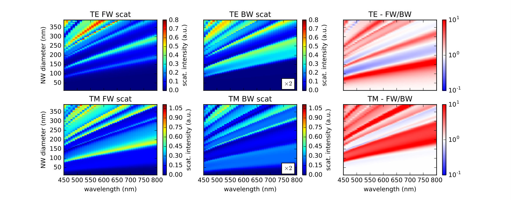 Figure 1
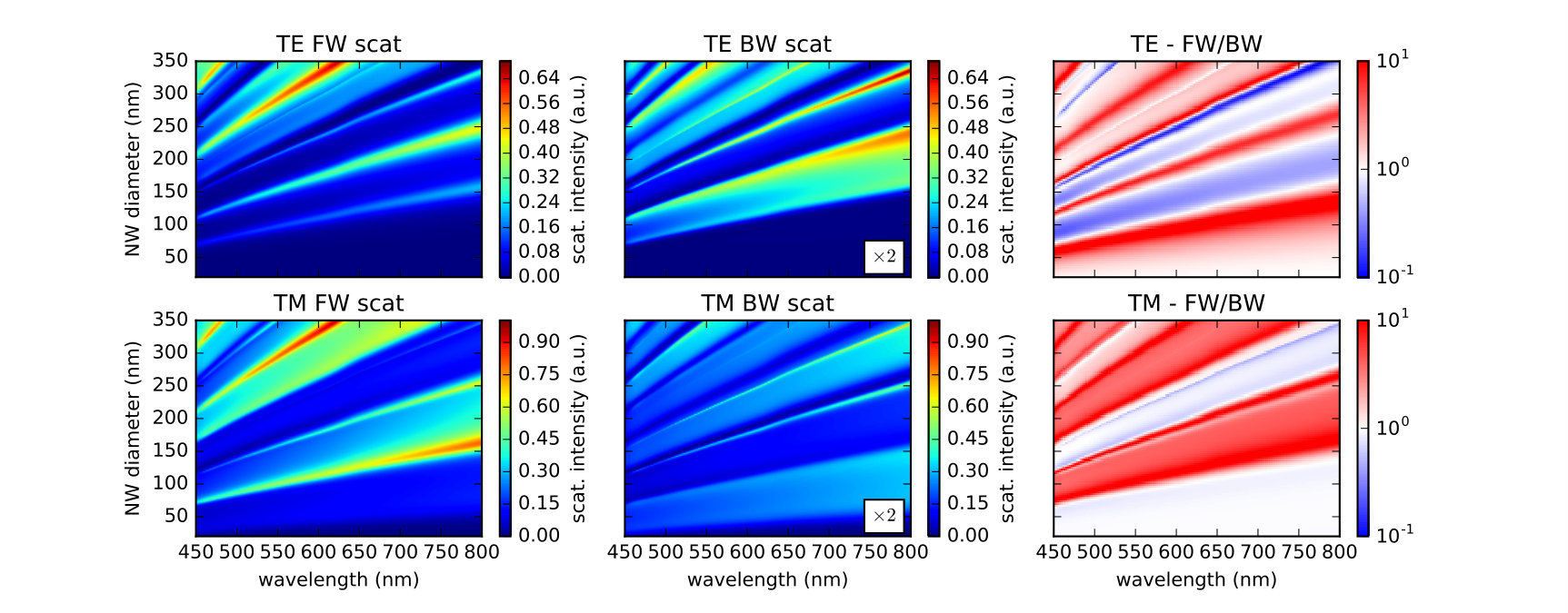 Figure 2
 Figure 3
 Figure 4
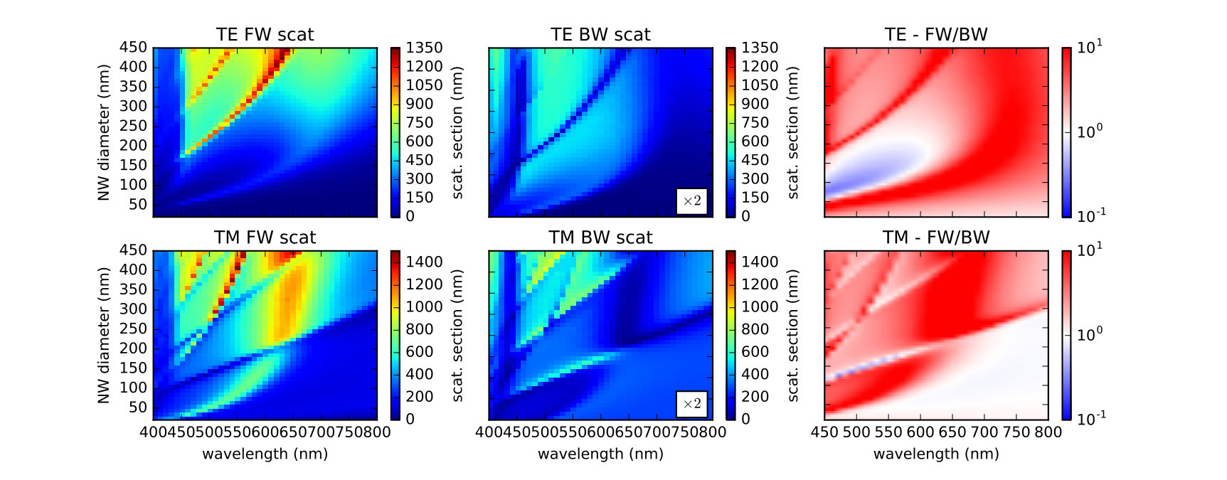 Figure 5
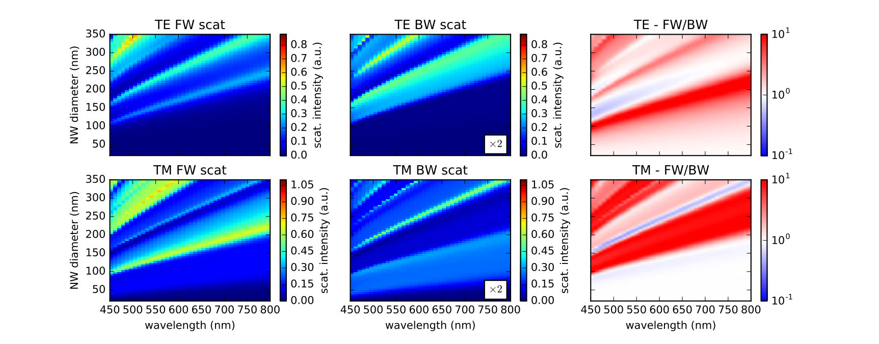 Figure 6
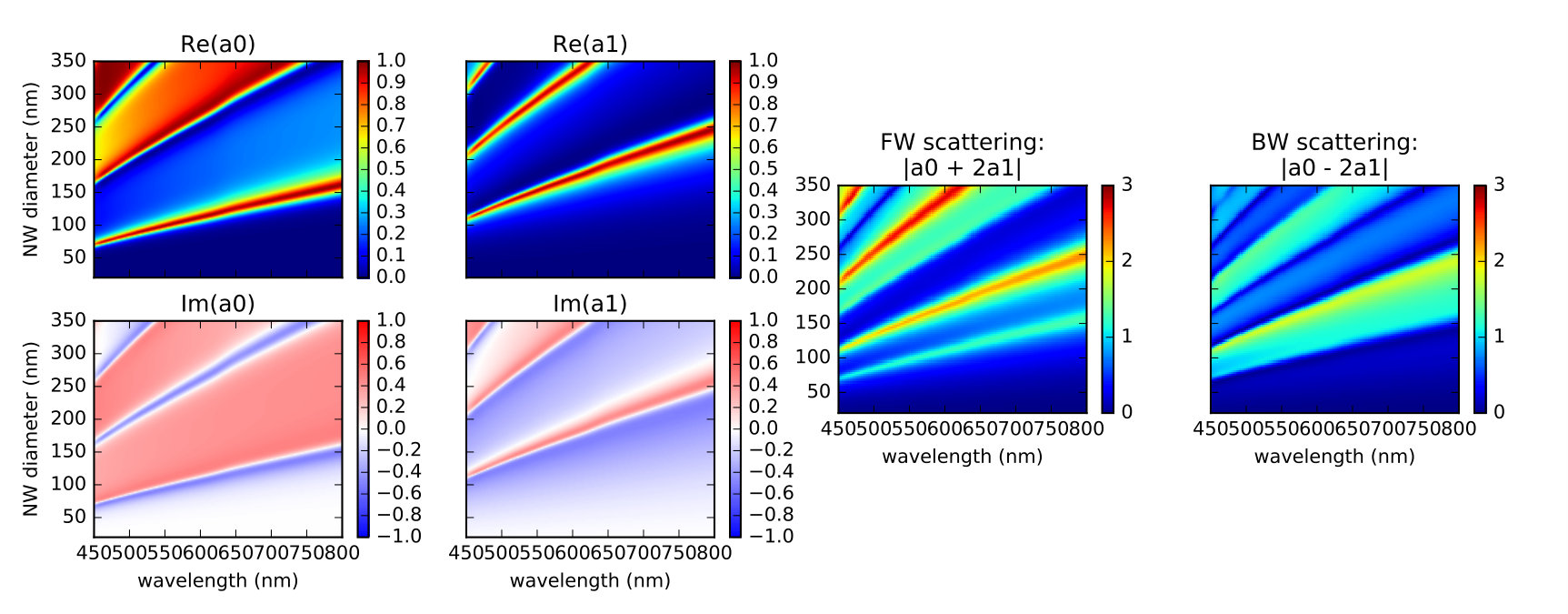 Figure 7
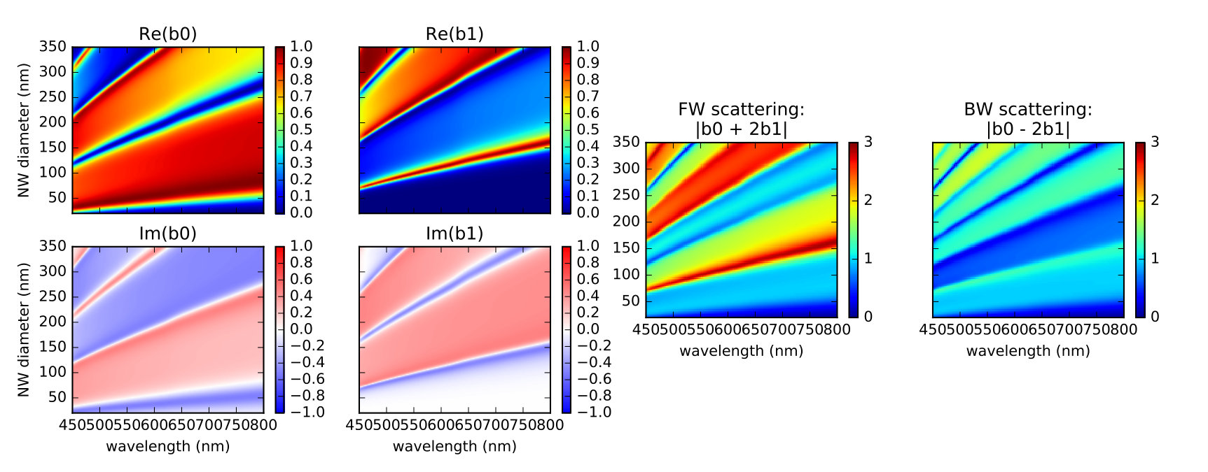 Figure 8
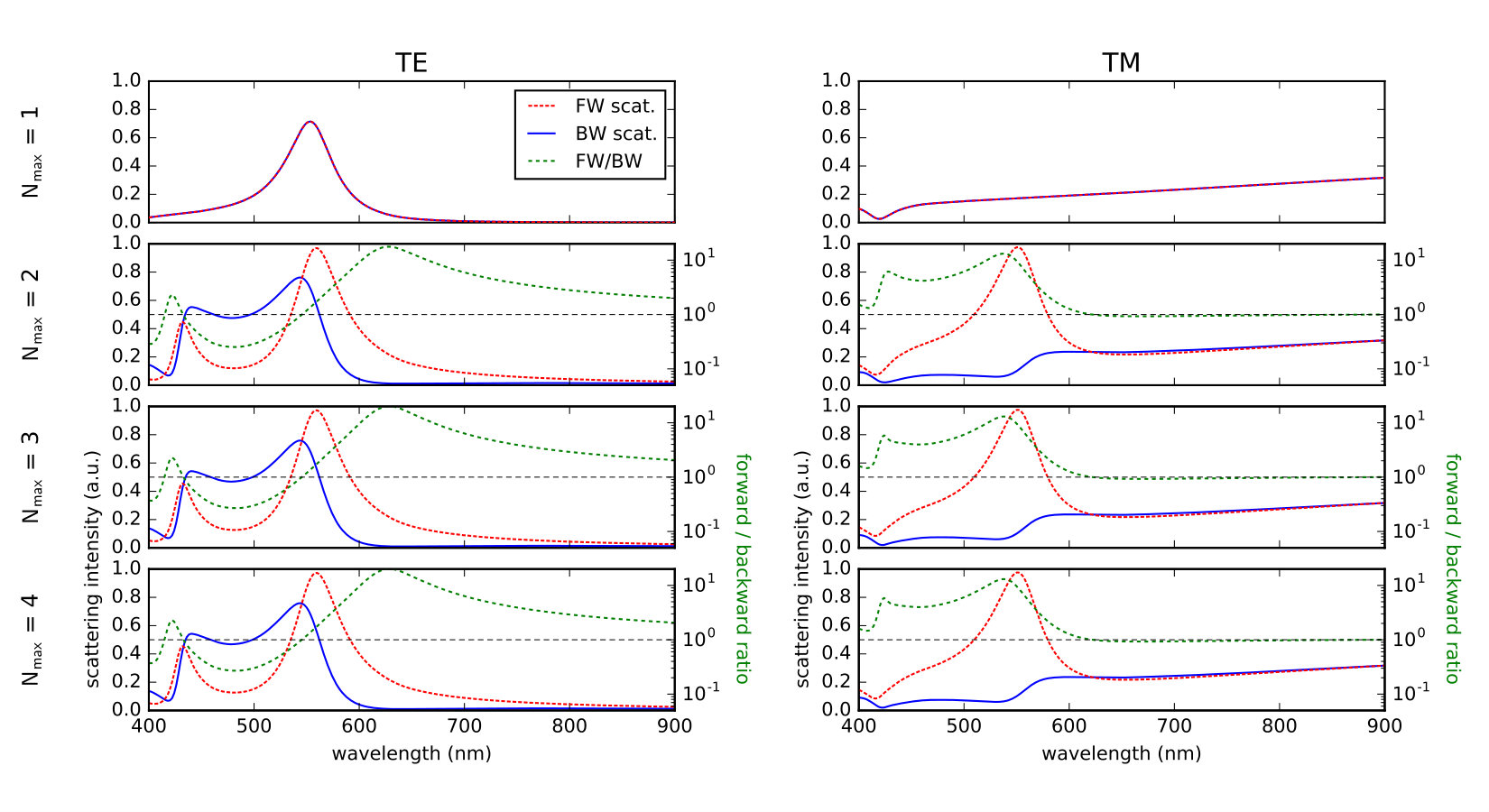 Figure 9
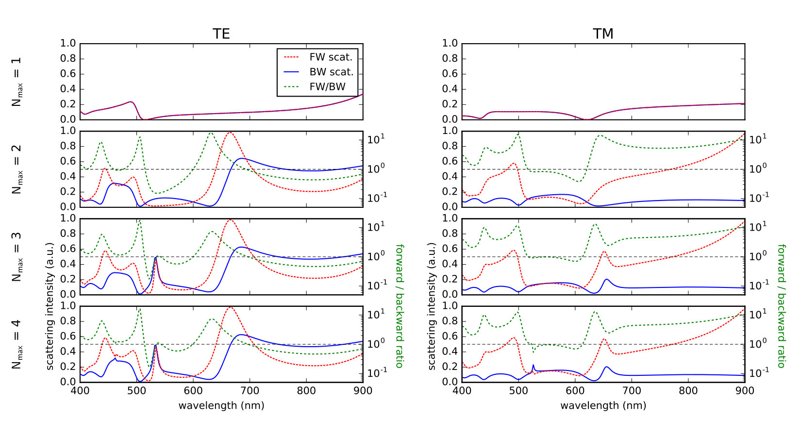 Figure 10
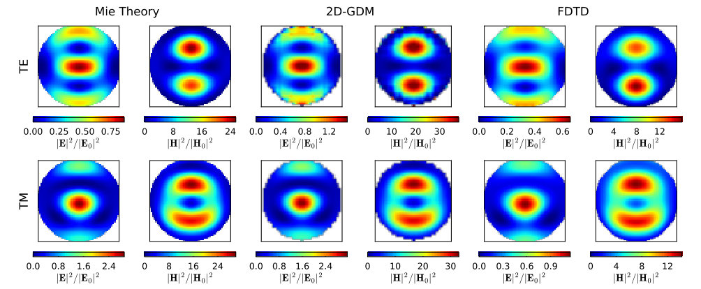 Figure 11
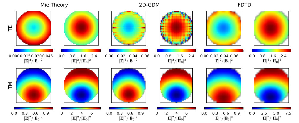 Figure 12
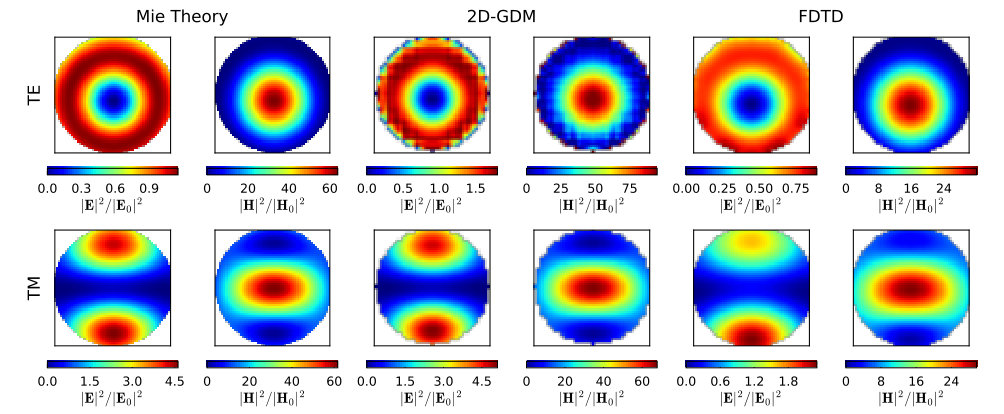 Figure 13
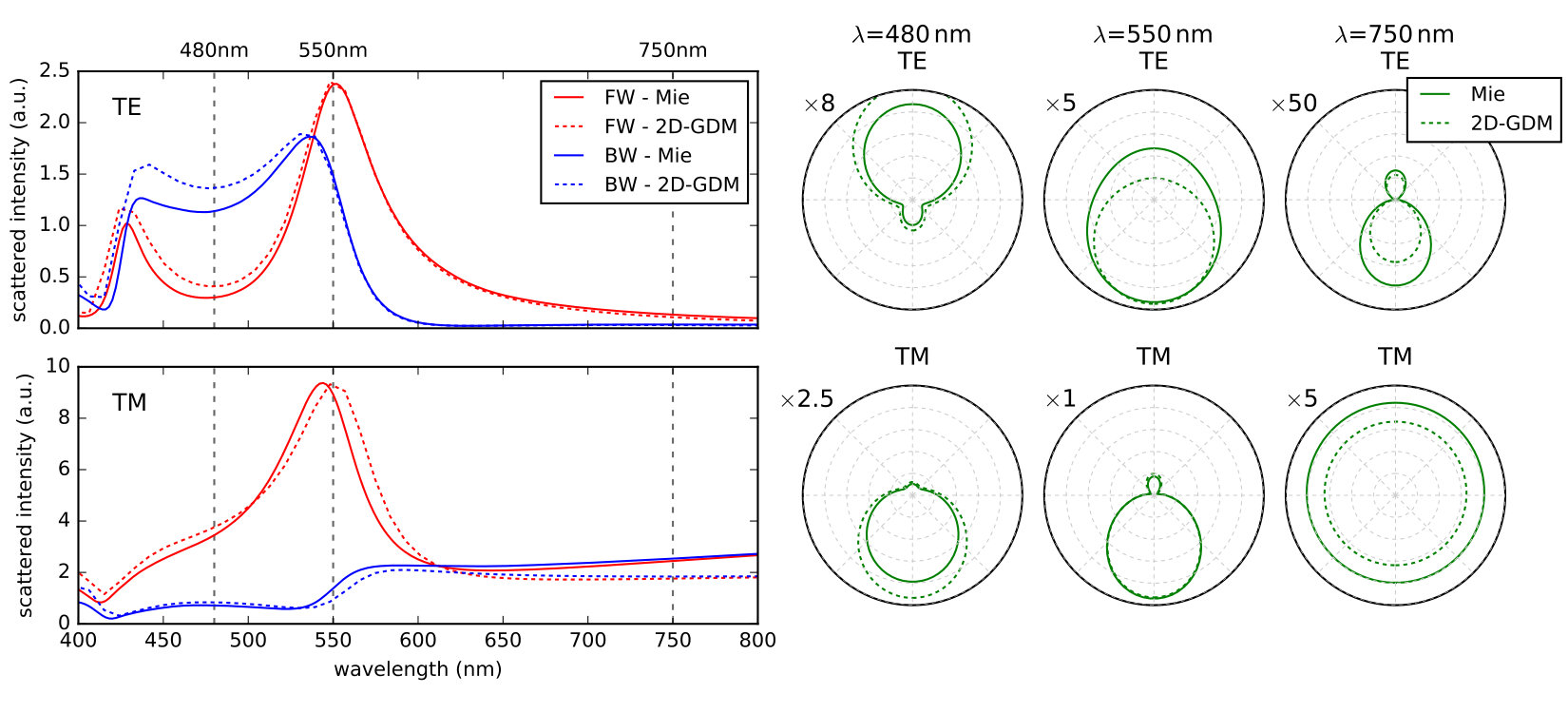 Figure 14
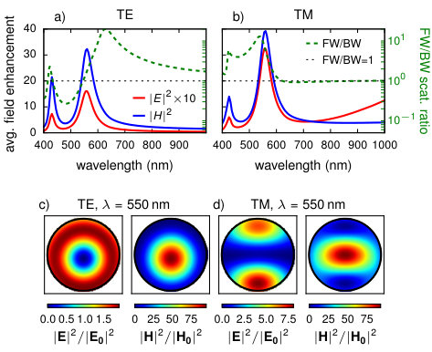 Figure 1
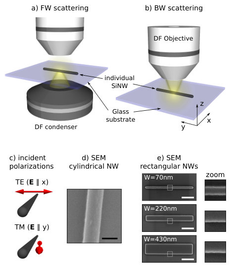 Figure 2
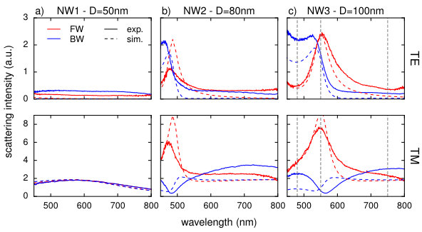 Figure 3
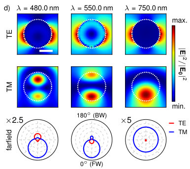 Figure 3
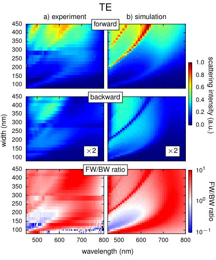 Figure 4
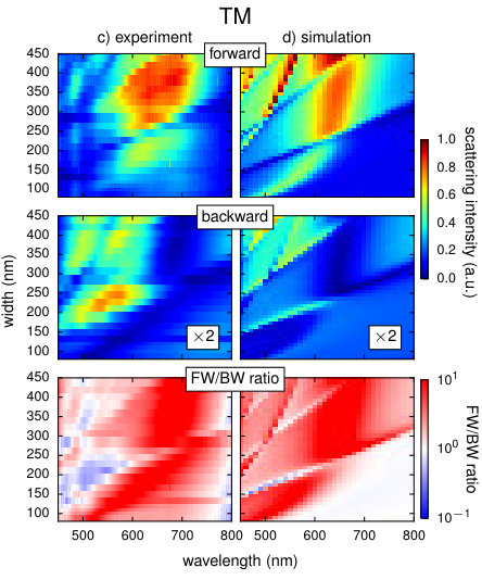 Figure 4
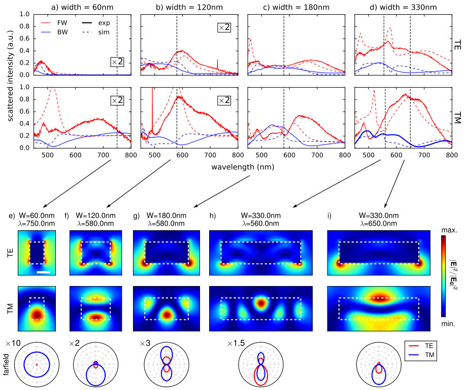 Figure 5
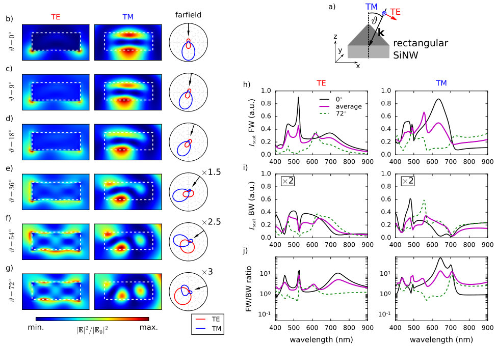 Figure 6
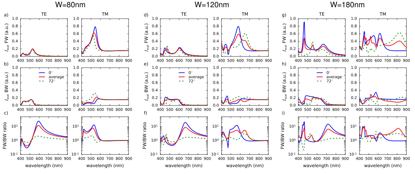 Figure 23
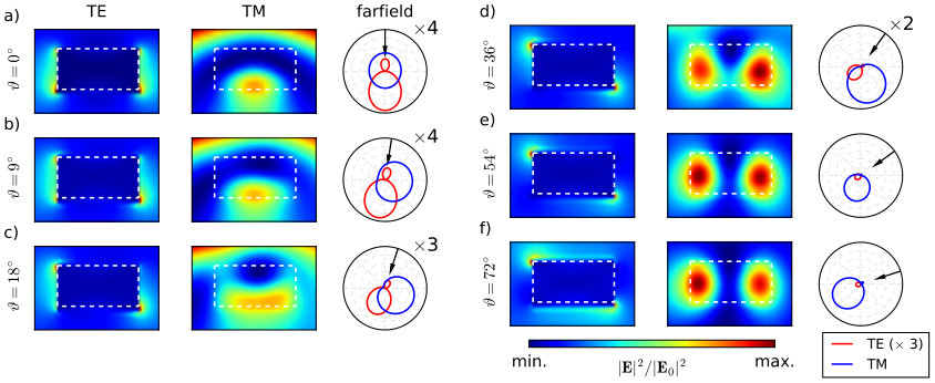 Figure 24
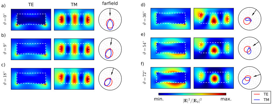 Figure 25
 Figure 26
 Figure 27
 Figure 28
 Figure 29
 Figure 30
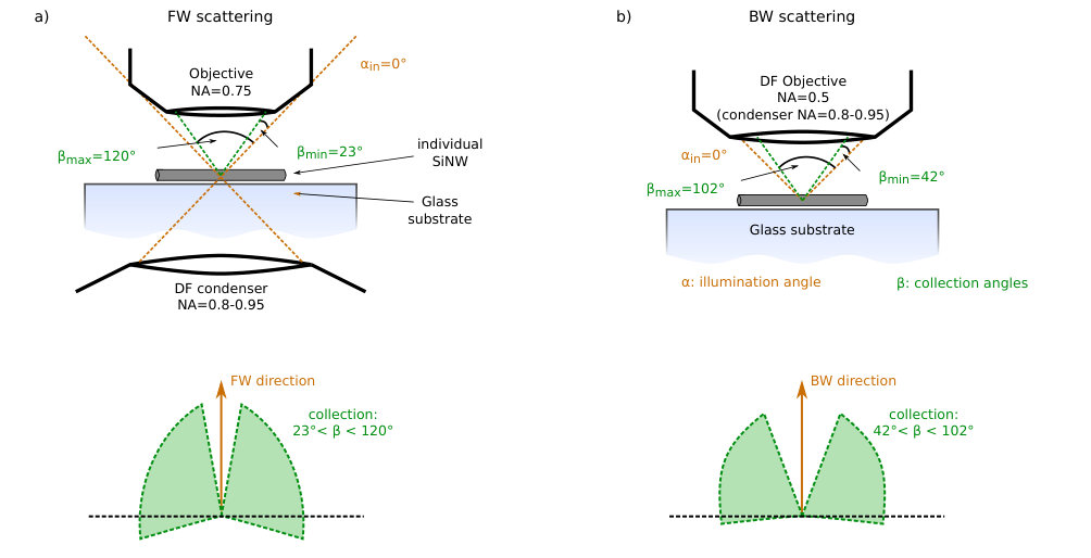 Figure 31
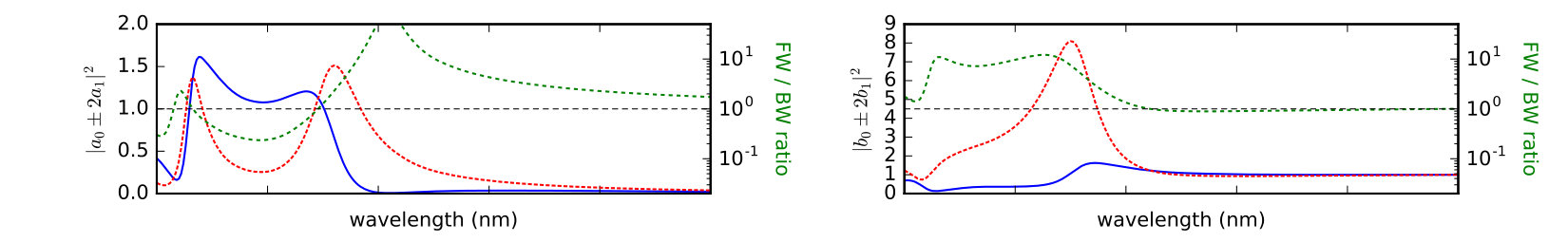 Figure 32
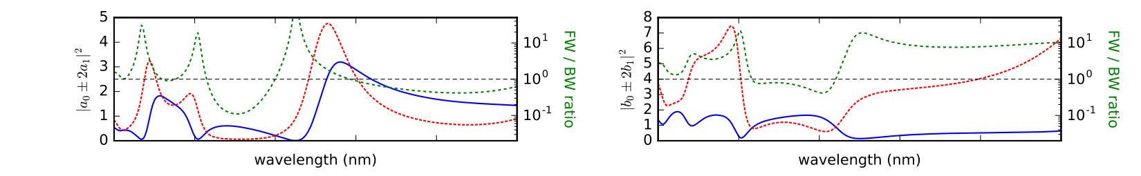 Figure 33
Peer Reviews
No public reviews on file for this paper yet. If you reviewed it on a platform where reviews are public (OpenReview, ICLR, NeurIPS, ICML), you can paste yours below so the community can read it here.
Videos
No videos yet. Explain this paper in a talk, walkthrough, or lecture? Add one.
Strongly directional scattering from dielectric nanowires
Peter R. Wiecha
CEMES-CNRS, Université de Toulouse, CNRS, UPS, Toulouse, France
Aurélien Cuche
CEMES-CNRS, Université de Toulouse, CNRS, UPS, Toulouse, France
Arnaud Arbouet
CEMES-CNRS, Université de Toulouse, CNRS, UPS, Toulouse, France
Christian Girard
CEMES-CNRS, Université de Toulouse, CNRS, UPS, Toulouse, France
Gérard Colas des Francs
ICB, UMR 6303 CNRS - Université Bourgogne-Franche Comté, Dijon, France
Aurélie Lecestre
LAAS-CNRS, Université de Toulouse, CNRS, INP, Toulouse, France
Guilhem Larrieu
LAAS-CNRS, Université de Toulouse, CNRS, INP, Toulouse, France
Frank Fournel
CEA-LETI/MINATEC, CEA, Grenoble, France
Vincent Larrey
CEA-LETI/MINATEC, CEA, Grenoble, France
Thierry Baron
CNRS, LTM, Université Grenoble Alpes, Grenoble, France
Vincent Paillard
CEMES-CNRS, Université de Toulouse, CNRS, UPS, Toulouse, France
Abstract
It has been experimentally demonstrated only recently that a simultaneous excitation of interfering electric and magnetic resonances can lead to uni-directional scattering of visible light in zero-dimensional dielectric nanoparticles. We show both theoretically and experimentally, that strongly anisotropic scattering also occurs in individual dielectric nanowires. The effect occurs even under either pure transverse electric or pure transverse magnetic polarized normal illumination. This allows for instance to toggle the scattering direction by a simple rotation of the incident polarization. Finally, we demonstrate that directional scattering is not limited to cylindrical cross-sections, but can be further tailored by varying the shape of the nanowires.
The search for ways to control light at subwavelength dimensions has increasingly attracted the interest of researchers for about the last two decades. Due to their strong polarizability and tunable plasmon resonances, metallic nanostructures are particularly suitable for the nanoscale manipulation of light – especially at visible frequencies.muhlschlegel_resonant_2005 However, such plasmonic structures suffer from certain drawbacks like strong dissipation associated to the large imaginary part of the dielectric function in metals.
Recently, dielectric nanostructures from high-index materials have proven to offer a promising alternative platform with far lower losses. kuznetsov_optically_2016 Like in plasmonics, it is possible to tune optical resonances from the near ultra-violet to the near infrared, yet with almost no dissipative losses. At these resonances, which can be of both electric or magnetic nature, strong local field enhancements bakker_magnetic_2015 and intense scattering kuznetsov_magnetic_2012 occur, tunable via the material and the geometry of the nanostructure. Prominent dielectric materials are, among others, silicon, germanium or III-V compound semiconductors with indirect band-gap. kallel_tunable_2012 ; albella_electric_2014 Conventional geometries include spherical nanoparticles kuznetsov_magnetic_2012 or nanowires (NWs), cao_tuning_2010 ; ee_shape-dependent_2015 but also more complex dielectric nanostructures wiecha_evolutionary_2017 . Dielectric optical antennas are promising candidates for applications in field-enhanced spectroscopy, gerard_strong_2008 ; wells_silicon_2012 ; regmi_all-dielectric_2016 ; cambiasso_bridging_2017 imaging, kallel_photoluminescence_2013 to enhance and control nonlinear effects shcherbakov_enhanced_2014 ; wiecha_enhanced_2015 ; wiecha_origin_2016 or to increase the efficiency in photovoltaics brongersma_light_2014 .
A peculiarity of dielectric particles is the possibility to simultaneously obtain a strong electric and magnetic response using very simple geometries. kuznetsov_magnetic_2012 ; bakker_magnetic_2015 ; mirzaei_electric_2015 ; valuckas_direct_2017 Recently, it has been independently shown by two research groups,person_demonstration_2013 ; fu_directional_2013 that exclusive forward (FW) or backward (BW) scattering, predicted by Kerker et al. in 1983 for hypothetical magneto-dielectric particles, kerker_electromagnetic_1983 can be realized in the visible spectral range using dielectric nanoparticles. Kerker et al. described two possible configurations, called the Kerker conditions. At the first Kerker condition zero backward scattering occurs for equal electric permittivity and magnetic permeability (). The second Kerker condition predicts zero forward scattering in small spherical particles when the first order magnetic and electric Mie coefficients are of equal absolute value and with opposite sign (). In contrast to particularly designed metamaterials,pendry_controlling_2006 the magnetic permeability is unitary in dielectric nanoparticles. Nevertheless, simultaneously occurring electric and magnetic resonances can de-facto fulfill the first Kerker condition. gomez-medina_electric_2011 ; nieto-vesperinas_angle-suppressed_2011 While the Kerker conditions were originally derived for spherical particles, it has been shown that the conditions are a result of a cylindrical symmetry and therefore can be generalized accordingly. zambrana-puyalto_duality_2013
Recent publications have confirmed the possibility to obtain optimum FW scattering also from elongated structures such as nanopillars, person_demonstration_2013 spheroids lukyanchuk_optimum_2015 or even from cuboidal dielectric particles ee_shape-dependent_2015 . Other dielectric particles on which directional scattering was investigated include nanodiscs for FW/BW directional metasurfaces, staude_tailoring_2013 ; decker_resonant_2016 patch antennas, yang_controlling_2015 V-shaped structures for multi-directional color routing, li_all-dielectric_2016 or asymmetric hollow nanodiscs for bi-anisotropic scattering alaee_all-dielectric_2015 , all of them based on the interplay between electric and magnetic modes. Control over the directional scattering can also be obtained using arrangements of nanoparticles like dimers albella_switchable_2015 ; campione_tailoring_2015 ; yan_directional_2015 or via hybrid metal/dielectric nano-structures guo_multipolar_2016 . Even directional shaping of nonlinear emission has been demonstrated: The radiation pattern of the third harmonic generation from silicon dimers can be controlled via the geometry of the structure. wang_shaping_2017 In a plasmonic-dielectric hybrid structure, the interplay of electric and magnetic resonances in dielectric TiO2 spheres was used to impose an uni-directional radiation pattern on the second harmonic generation from a plasmonic driver element.xiong_compact_2016
Compared to zero-dimensional (0D) particles of deeply sub-wavelength size in all directions (like nano-spheres), one-dimensional (1D) nanowires have a strongly polarization dependent optical response, which offers an additional degree of freedom, supplementary to the choice of material and modifications of the nano-structure’s geometry. Despite this opportunity, research on directional scattering from dielectric nanowires is still scarce. As for scattering, it has been shown theoretically that multi-layer dielectric mirzaei_all-dielectric_2015 or plasmonic-dielectric core-shell liu_invisible_2015 nanowires can be rendered invisible by tailoring destructive interference between different order modes or electric and toroidal dipole modes, respectively. Such entities might be useful for cloaking applications, for instance to create “invisible” electric contacts or circuits. fan_invisible_2012 Dense arrays of vertical dielectric NWs on the other hand, possess a strong light extinction due to multiple scattering inside the nanowire assembly, which can be used as an anti-reflection coating for photovoltaics.grzela_polarization-dependent_2012 ; muskens_design_2008 At the level of an individual nanowire, angle-dependent absorption can be tailored via the incident angle through the interplay between Mie-type and guided modes.abujetas_unraveling_2015 Also, the directionality of photoluminescence from individual III-V nanowires can be tailored through the supported Mie and guided modes grzela_nanowire_2012 ; paniagua-dominguez_enhanced_2013 ; brenny_directional_2016 .
In contrast to these former works on complex geometries or effects, in this paper we study the directional scattering of light from individual normally illuminated dielectric nanowires. Using Mie theory we analyze in a first step the interplay of different order Mie modes, leading to the occurrence of directional scattering. We then compare experimental results from individual, single crystal silicon nanowires (SiNWs) of cylindrical and rectangular cross-sections. In both cases spectral zones of strongly anisotropic FW/BW scattering ratios can be identified and we find that asymmetric wire geometries allow even further tailoring of directional scattering and offer the incident angle of the illumination as a supplementary free parameter. We confront our experimental results with simulations using the Green dyadic method (GDM), yielding a very good agreement.
I Directional scattering from cylindrical nanowires
Mie theory can be applied to infinitely long cylinders by expanding the fields in vector cylindrical harmonics. The Mie scattering coefficients and of the expansion can be regarded as weights for corresponding electric and magnetic multipole moments, representing the response of the wire to an external illumination. Under normal incidence, the Mie S-matrix, connecting the incident () and the asymptotic, scattered field () writesBohren and Huffman (1998)
[TABLE]
with the wavenumber , the distance to the cylinder axis and
[TABLE]
is the scattering angle with respect to the incident wave vector and corresponds to the forward scattering direction.
As can be seen from Eq. (1), under normal incidence the transverse magnetic (TM) and transverse electric (TE) polarized components of the scattered fields are proportional to the S-matrix components , respectively . Therefore, according to Eqs. (2) scattering from a TE polarized normally incident plane wave ( NW axis) is only due to the “electric” multipole contributions . On the other hand, a TM polarized illumination ( NW axis) induces scattering exclusively via the “magnetic” Mie terms . The expressions “electric” and “magnetic” refer to the fact that in the TE and TM case, the magnetic, respectively electric field components are zero in the scattering plane.
Let us now consider the case of sufficiently small nanowires, where only the first two orders of the Mie expansion contribute significantly to scattering. For SiNWs in the visible spectral range, this assumption is a good approximation for diameters up to at least nm (see also supporting informations (SI), Figs. S1-S2). By setting or in equations (2) we obtain the conditions for zero scattering in forward (FW), respectively backward (BW) direction. For TM polarized illumination we find:
[TABLE]
The same conditions hold for and in the TE configuration. Hence if the conditions in Eqs. (3) are met, it is possible to obtain uni-directional scattering from 1D dielectric nanowires, which is the result of interference between the simultaneously excited first two multipole contributions. In figure 1(a-b), the FW/BW scattering ratio is shown (dashed green lines) for a SiNW of diameter nm for (a) TE and (b) TM polarized excitation, revealing zones of strongly directional scattering. For the dispersion of silicon we use tabulated data from Ref. Edwards, 1997 throughout this paper. In the SI Figs S3-S4 we show the first two order Mie coefficients for SiNWs as function of the wavelength and the nanowire diameter and find that zones where the conditions in Eqs. (3) are approached do exist at several wavelength / diameter combinations for normally illuminated cylindrical silicon nanowires.
We want to note that a similar derivation has been performed for core / shell metal / dielectric nanowires, where the plasmonic core was introduced in the NW to shift the electric and magnetic dipolar modes to spectrally overlap, leading to directional scattering effects. liu_scattering_2013 In contrast to this former theoretical work, we study interference between different order multipole contributions in homogeneous dielectric nanowires, leading to strongly directional scattering even in such very simple systems.
It is possible to expand the electromagnetic fields inside the cylinder in the same way as the scattered fields of Eq. (1). For details, we refer to the textbook of Bohren and Huffmann (chapters 4 and 8.4).Bohren and Huffman (1998) In figure 1 the average internal field intensity enhancement is shown for a SiNW with diameter nm with a TE (a) and TM (b) polarized incident plane wave, respectively. Interestingly, at the resonant wavelengths we observe not only high electric field intensities (red lines) but also a very strong enhancement of the magnetic field (blue lines), regardless of the incident polarization orientation. For both polarizations, the magnetic field increases even significantly stronger compared to the electric field intensity. We remark that this observation is in agreement with recent results from dielectric cylinders in the GHz regime.kapitanova_giant_2017 We conclude that a simultaneous excitation of strong electric and magnetic fields occurs in dielectric, non-magnetic (i.e. ) nanowires, even under pure TE or TM polarized illumination and normal incidence. Hence, in analogy to the findings of Kerker et al. for the case of spherical dielectric nanoparticles, the observed directionality (dashed green lines in Fig. 1) can be interpreted as a result of the interference between “effective” electric and magnetic modes. In particular, no directional scattering is obtained at the non-degenerate, fundamental TM01 mode, where only the internal electric field shows a resonant enhancement while the magnetic field intensity follows a flat line beyond nm (see Fig. 1b). For illustration the electric and magnetic field intensity patterns inside the NW cross section are shown for an incident wavelength nm in Fig. 1(c-d).
II Spectroscopy on cylindrical silicon nanowires
In order to compare the forward and backward scattering of a normally incident plane wave on silicon nanowires (SiNWs) we perform standard darkfield microscopy either in reflection (backward scattering, “BW”) or in transmission geometry (forward scattering, “FW”). The measurement geometry is schematically shown in Fig. 2(a) and (b) for FW and BW scattering, respectively. For details on the measurement technique, see Methods. We compare our experimental results to 2D simulations (in -plane, assuming infinitely long structures along ) by the Green dyadic method. Likewise, the GDM simulation technique is explained in the methods section. In the SI Figs. S5-S10, the accuracy of the method is verified by comparing GDM simulations to Mie theory and FDTD simulations.
We measure the scattering from cylindrical SiNWs of diameters between nm and nm, epitaxially grown by the vapor-liquid-solid (VLS) technique and drop-coated on a transparent glass substrate. The NW size-dispersion was obtained via scanning electron microscopy (SEM) from a second sample consisting of the same SiNWs, drop-coated on a silicon substrate (see Fig. 2d). For details, see the methods section. Results of the scattering experiments are shown in Fig. 3(a-c) for TE (top row) and TM (bottom row) polarized illumination. The given NW diameters are estimates, obtained by comparison with simulations.
The very weak (TE), respectively omnidirectional (TM) scattering in case of the the smallest nanowire (Fig. 3a, NW1: nm) is in perfect agreement with the GDM simulations and confirms the assumption of a purely dipolar response if only the non-degenerate TM01 mode is excited (see also field plot for nm in figure 3d on the right). As expected, with increasing NW diameter (figure 3b-c), we observe a simultaneous red-shift of the FW and BW scattering peaks. For the largest SiNWs (Fig. 3c, nm), in the case of TE polarized illumination mainly FW scattering occurs in a limited spectral range (nm), before BW scattering takes over at shorter wavelengths (nm). Note that around nm, we obtain the possibility to invert the main scattering direction by simply flipping the polarization from TM to TE (see Fig. 3d, bottom left or also SI, Fig. S5). By changing the NW diameter this spectral zone can be also tuned to other wavelengths (see SI, Figs. S6-S7). At longer wavelengths (nm), only the TM01 mode exists, leading to very weak overall scattering under TE incidence and to the above mentioned, omnidirectional radiation pattern in the TM geometry. Interestingly, while TE excitation can induce uni-directional BW scattering, under TM polarization BW scattering is generally very weak and mainly FW scattering occurs as soon as higher order contributions are excited together with the TM01 mode.
In summary, we note that although we do observe BW scattering (mainly under TE polarization) it mostly remains weak compared to the FW scattered light. This has been also observed in the case of 0D-particlesfu_directional_2013 ; yan_directional_2015 and can be explained with the finding that the second Kerker’s condition (describing BW scattering) is contradicting the optical theorem and thus cannot be exactly fulfilled. alu_how_2010 Furthermore it is difficult to even closely meet the second condition.zambrana-puyalto_duality_2013 In the case of TM polarized illumination, the FW/BW scattering ratio is even almost exclusively (see also SI, Figs. S5-S7 for more simulations on cylindrical NWs).
III Asymmetric, Rectangular Silicon Nanowires
In a second step we analyze what happens if the cylindrical symmetry of the nanowire cross section is broken. We therefore fabricate SiNWs of rectangular section by electron beam lithography (EBL) and subsequent dry-etching on a silicon-on-quartz (SOQ) substrate. For details on the fabrication process, see Methods. We want to point out a great advantage of our top-down approach on SOQ: The possibility to create silicon nanostructures of arbitrary shape by EBL on a transparent substrate from single crystalline silicon. Using crystalline material rather than polycrystalline or amorphous silicon guarantees that the high refractive index of silicon is obtained and facilitates furthermore the modeling, since accurate tabulated data for the dispersion is available in literature.Edwards (1997) This gives us the opportunity for a systematic analysis of the scattering from rectangular SiNWs of variable width. The height of the structures however remains constant, defined by the thickness of the silicon layer on the SOQ substrate (nm in our case). We choose SiNWs with length long compared to the focal spot of the illuminating optics (all data acquired on NWs with µm) in order to obtain a purely Mie-like response.traviss_antenna_2015 SEM images of selected rectangular SiNWs are shown in figure 2e. The images are obtained from a second sample, fabricated with the exact same process parameters but on a non-insulating silicon-on-insulator (SOI) substrate. For the purpose of better illustration NWs of µm length are shown. We point out that all NWs have excellent surface properties, low roughness and steep flanks.
The results of our systematic FW/BW scattering measurements are shown in figure 4. Spectra for TE polarized illumination are shown in (a-b), TM spectra in (c-d). The comparison of experiments ( (a) and (c) ) with GDM simulations ( (b) and (d) ) show a very good qualitative and quantitative agreement. Having a look at the FW/BW ratios (Fig. 4, bottom row) we observe that uni-directional scattering occurs mostly towards the FW direction. Spectrally relatively narrow peaks of strong forward scattering can be identified for both, TE and TM polarized illumination. On the other hand, a zone of significant BW scattering is observed only in the case of TE polarization, similar to our observations on cylindrical SiNWs.
Selected spectra from Fig. 4, as well as several near-field intensity plots are shown in figure 5. The spectra in (a-d) confirm the very good agreement between experiment (solid lines) and simulations (dashed lines). For the smallest nanowire widths as well as for long wavelengths, we find again an omnidirectional scattering, corresponding to a purely dipolar response (Fig. 5e). In analogy to cylindrical NWs, this first order resonance can only be excited in the TM geometry, TE polarized illumination results in a very weak scattering in the corresponding spectral range. While small nanowires have spectrally broad optical resonances (figure 5a-b), narrower higher order resonances appear with increasing NW width (figure 5c-d). In contrast to the omnidirectional TM scattering in the smallest wires, the first occurrences of strong forward scattering seem to be the result of interference between a sharp quadrupolar resonance and a broad dipolar contribution. We deduce this conclusion from the similarity in field intensity distributions in cylindrical and rectangular NWs (compare Figs. 3d and 5e,f,i).
Under TM excitation, we also observe branches of a different kind of Fano-like resonances where the FW/BW ratio is almost unity (see Fig. 4c-d and Fig. 5c-d, bottom row). In a narrow spectral window the otherwise strong forward scattering is suddenly suppressed while BW scattering increases. Resonances with such field profiles are observed neither under TE polarization, nor in symmetric SiNWs (see SI Figs. S11-S15, where scattering from rectangular wires is compared to different symmetric geometries). We attribute these sharp features to horizontal guided modes along the SiNW width (-direction), the wire side facets acting as the Fabry-Perot cavity mirrors. To verify this assumption we assess the effective index for the supported guided mode(s) assuming a 1D waveguide of infinite extensions in - and -direction. For the case of TM polarized illumination at nm, the corresponding first order guided mode along the width of the NW has an effective index of (). The first and second order standing wave patters in figure 5g and h match perfectly with the nanowire widths of nm, respectively nm (at nm for the latter). For more details on the supported guided modes, see section V in the SI. It is possible to exploit these Fabry-Perot like modes in order to toggle between FW and omni-directional scattering within a narrow spectral window – simply by switching the incident polarization from TE to TM (see e.g. around nm in figure 5d).
Figs. 5(g-h) (TM: center row) correspond to near-field intensity distributions inside the SiNW at the first two orders of these TM-excited Fabry-Perot resonances. The field patterns inside the NW cross section correspond indeed to standing wave patterns of guided modes, which eventually lead to an almost equal FW and BW scattering in a narrow spectral region (see Fig. 5(c-d) bottom, ). We remark that the assumption of spectrally sharp, guided modes between the NW side facets is also in agreement with former studies on scattering from rectangular dielectric NWs.fan_optical_2014 ; landreman_fabry-perot_2016
Finally, we want to assess the influence of non-normal illumination on FW and BW scattering from rectangular SiNWs. For spectroscopy on single nanowires, we need to use a high-NA microscope objective, which results in a large dispersion of incident angles, with angles up to in our setups (NA , see also Methods). In figure 6, we show simulated field intensity distributions in the scattering plane and scattering spectra for a rectangular SiNW of nm width (height nm) for different incident angles (depicted in figure 6a). To calculate the spectra, while the angle of incidence is varied, we fix the integration solid angle to the upper (BW) and lower (FW) hemisphere, corresponding to a fixed position of the collecting microscope objective. The wavelength in (b-g) is nm, the electric field is either polarized parallel to the scattering plane (TE) or along the NW axis (TM). (b-g) show the field intensity and angular farfield intensity patterns in the NW section for increasing incident angles.
We observe, that while the original field distribution can still be recognized for angles up to , at high angles the nearfield distribution as well as the farfield radiation pattern are completely different. In (h-j) we show FW scattering (h), BW scattering (i) and FW/BW ratio (j) spectra for the same rectangular SiNW. The black lines correspond to normal incidence and the green dashed lines to an incident angle of . The magenta lines denote the average scattering for illumination angles from to , hence an approximation to our experimental conditions. The spectra for an illumination angle corresponding to NA 0.95 show often even completely opposite trends compared to normal incidence. In (j) for instance regions exist where the directionality flips from FW under normal incidence to BW for an angle of . On the other hand, the spectra calculated using the average illumination angles follow the trends of normal incidence.
We conclude, that a normally incident plane wave gives a valid first-order approximation even for rectangular NWs illuminated by tightly focused beams. This is also supported by the good agreement between normal-incident simulations and the experimental data (see figure 4). In the SI Figs. S17-S19, we show nearfield intensity maps for different excitation wavelengths and nanowire geometries as well as further spectra for comparison with figure 5, confirming the trends discussed above. In the supporting informations, we also discuss a selected example, where the normal incidence approximation breaks down.
IV Conclusions
In conclusion, we demonstrated strongly directional light scattering from symmetric an asymmetric dielectric nanowires at optical frequencies. We derived the conditions for exclusive forward or backward scattering in cylindrical nanowires from Mie theory and showed both theoretically and experimentally that anisotropic scattering can be obtained from individual silicon nanowires. Unlike 0D-structures, directionality is a result of interference between different orders of either transverse electric or -magnetic modes. Also, compared to 0D nano-particles the incident light polarization offers an additional degree of freedom in nanowires – apart from material and geometry variations. Besides being able to adjust the scattering intensity, the directionality and the spectral width of the resonances by varying the NW width, it is for example possible to switch between FW and BW scattering simply by rotating the polarization of the incident light. Finally we showed that by breaking the symmetry of cylindrical nanowires and using rectangular cross sections instead, Fano-like resonances occur, leading to spectrally very sharp features with unity FW/BW scattering ratio, due to guided modes along the NW width. Again, this isotropic scattering can be triggered by switching the incident polarization between TE and TM. We demonstrated that asymmetric nanowires also allow to tune the scattering response via the angle of incidence. Our results open perspectives for various applications where spectrally tunable directional guiding of light is required at a nano scale, for instance in optical nano-circuits. Furthermore, dielectric nanowires may be used for example for anisotropic cloaking purposes, hence observer-dependent invisibility, in wavelength-selective field-enhanced spectroscopies or for directional non-linear emission. Finally, due to the simplicity of the silicon nanowires and their compatibility with production-ready technology, our results render nanowires very interesting for light harvesting applications in photovoltaics.
V Methods
V.1 Crystal Growth of Cylindrical SiNWs
The cylindrical silicon nanowires were grown in a hot-wall reduced pressure chemical vapor deposition system via the Vapor-Liquid-Solid (VLS) process. Au droplets were used as catalysts, their sizes can be easily controlled and define the diameter of the nanowires. The reactor pressure was Torr, as precursor for the Si growth silane (SiH4) was used, diluted with hydrogen as carrier gas. More details can be found in reference dhalluin_silicon_2010, . Subsequent to the expitaxy, the grown SiNWs were removed from the substrate by careful sonication in isopropyl alcohol solution. For the scattering experiments the NWs were finally drop-coated onto a transparent glass substrate with lithographic markers. A second sample was prepared on a silicon substrate for scanning electron microscopy, on which we determined a dispersion in NW diameters between around nm and nm.
V.2 Lithographic SiNWs by Electron Beam Lithography on Silicon on Quartz Substrates
The so-called silicon-on-quartz (SOQ) substrates were fabricated starting from commercially available SOI substrates. A first thinning step is realized by thermal oxidation and oxide removal in order to adjust the top silicon thicknesses according to specifications. Direct bonding is then performed to join the SOI to fused silica substrates. As silicon and silica present a large CTE mismatch (CTE: Coefficient of thermal expansion), high thermal processes are prohibited to improve the bonding strength and the annealing temperature is therefore limited to C. moriceau_materials_2014 This implies dedicated surface preparation to achieve high adherence energy at low temperature: SOI are prepared with a nitrogen plasma and the fused silica with a chemical mechanical process step. The bonded structure is then thinned by grinding and chemical etching in order to remove the base silicon substrate as well as the buried oxide layer (BOX).
The rectangular NWs were fabricated by a top-down technique via electron beam lithography (EBL) and subsequent anisotropic plasma etching. han_realization_2011 ; guerfi_high_2013 A transparent SOQ wafer with a nm thick Si overlayer served as substrate. A RAITH 150 writer at an energy of 30 keV was used for EBL, employing a thin (60nm) negative-tone resist layer (hydrogen silsesquioxane, “HSQ”). After the EBL step, HSQ was developed by immersion in % tetramethylammonium hydroxide (TMAH) for min. The patterns in the resist were finally written into the SOQ silicon top layer by reactive ion etching (RIE). For the RIE step, a SF6/C4F8 plasma was used. Etching was stopped when the silica layer was reached, following in-situ analysis. A residual layer of nm of SiO2 (developed resist) remains on the structures, which has no major impact on the optical properties due to its low index and small thickness. A comparison with a sample where the residual layer was removed using fluorhydric acid showed no significant difference in the spectra, but smaller structures were destroyed due to under-etching.
For SEM imaging, a second sample was prepared with identical process parameters on a silicon on insulator (SOI) substrate (Si-Layer: nm, BOX layer: nm)
V.3 Forward/Backward Confocal Darkfield Spectroscopy
Forward, “FW”:
Transmission confocal optical dark-field (DF) microscopy was performed on an inverted optical microscope. A broadband white lamp was focused through the sample substrate on the individual SiNWs using a DF condenser (Nikon, NA ). The FW scattered light was collected using a Nikon NA microscope objective, spatially selected via a confocal hole and guided through a polarization filter ( or to the NW axis for TM and TE geometry, respectively). Finally, the light was dispersed by a grooves per mm grating on a highly sensitive CCD (Andor Newton).
Backward, “BW”:
Reflection confocal optical DF experiments were carried out on a separate spectrometer (Horiba XploRA). A white lamp was focused on individual SiNWs by a dark-field objective (NA , condenser: NA ). The backscattered light was filtered by a confocal hole and a polarization filter and dispersed by a grooves per mm grating on a highly sensitive CCD (Andor iDus 401).
In both setups (FW and BW), for practical reasons we put the polarization filters in the detection path (detection direction normal to the NW axis). Because we limit our investigations to normal illumination (no depolarization) and due to the linearity of the fields, we assume that the polarization filter after the sample is equivalent to a polarized, normal incidence.
Normalization:
In the FW as well as in the BW scattering experiments, the intensity distribution of the respective lamp as well as the spectral response of the optical components was accounted for by the following normalization scheme: First, the background noise was substracted (DF measurement on the bare SOQ / glass substrate). Subsequently the data was normalized using the spectra of the respective lamps, measured through the bare substrate (“FW” setup) and via a white reference sample (“BW” setup). Since we measure FW and BW scattering on two entirely different setups, we cannot compare the spectra quantitatively. Therefore we use the scattering from the smallest cylindrical nanowire (“NW1”, nm, Fig. 3a bottom) for normalization of the data between the two measurement geometries: In sufficiently small NWs illuminated by TM polarized light, exclusively the fundamental dipolar TM01 mode is excited. This results in an omni-directional scattering, corresponding to a dipolar source along the SiNW axis. Thus we can assume that the FW and BW scattered intensities under these conditions are of equal strength and normalize all spectra according to this reference.
Incident and detection angles:
The upper limit for the incident angle from the dark-field condensers (FW and BW both ) is
[TABLE]
The high incident angles can modify the response of the Mie resonances. However, since the illumination is conic, only a fraction of the incident light has actually a large wavevector component parallel to the nanowire . Thus, assuming normally incident plane wave illumination in the simulations is a valid approximation to our experimental conditions, further justified by the excellent agreement between our simulations and measurements.
The upper limits of the detection angles can be calculated by the collecting objectives’ numerical apertures:
[TABLE]
With the maximum incident angle this eventually leads to the following angular detection ranges (per polar quadrant):
[TABLE]
The simulated range is . Given the excellent agreement between simulations and measurements, the deviations between the collection angles seem not to cause a serious problem. We attribute this to the fact that scattering is either omni-directional or else strongly forward/backward directional. In both cases, large angles with respect to the incident wave-vector direction contribute only weakly to the total scattering.
See also SI, Fig. S16 for a detailed sketch, illustrating the collection angles.
V.4 GDM Simulations
Because of the high aspect ratio of the nanowires, we assume infinitely long structures (NW axis along ). In this manner we simplify the computation to a two dimensional (2D) problem. The electric field is calculated using the Green dyadic method (GDM). Practically, we solve the vectorial Lippman Schwinger equation
[TABLE]
at the frequency , by discretizing the nanostructure using square meshes. and are the incident field and resulting field inside the nanostructure, respectively. is the Green’s dyad and the electric susceptibility of the structure material (). is the incident wavevector along the NW axis. For normal incidence, . The integral in Eq. (7) runs over the surface of the 2D particle cross section. This self-consistent equation is solved (e.g. using standard LU decomposition) and the field can be computed in the nanowire. Knowing the field inside the nanostructure, application of Eq. (7) permits to compute the field everywhere, both in the near-field and far-field zone. For details we refer the interested reader to Refs. Martin et al., 1995 and Paulus and Martin, 2001.
All simulations are carried out for SiNWs in vacuum () to allow direct comparison with Mie theory for the cylindrical wires (see SI, Figs. S5-S10). Given the large index contrast with silicon ( in the visible), this is a good approximation, which is supported also by the excellent agreement between simulations and measurements.
Acknowledgements.
This work was supported by Programme Investissements d’Avenir under the program ANR-11-IDEX-0002-02, reference ANR-10-LABX-0037-NEXT, by LAAS-CNRS micro and nanotechnologies platform member of the French RENATECH network, by the Région Midi-Pyrénées and by the computing facility center CALMIP of the University of Toulouse under grant P12167.
Supporting Informations
In the supporting informations we show further details on FW/BW scattering from nanowires by Mie theory as well as additional simulations.
Notes
We note that a similar, theoretical work has been published during the review of this manuscript, describing scattering phenomena in nanowires with a radially anisotropic refractive index.liu_superscattering_2017
The authors declare no competing financial interest.
Supporting informations: Strongly directional scattering from dielectric nanowires
I Contributing Mie orders to FW/BW scattering intensity
Mie theory can be applied to infinitely long cylinders by expanding the fields in vector cylindrical harmonics (instead of the vector spherical harmonics as in “classical” Mie theory for spherical particles). The expansion coefficients for the scattered fields are the so-called scattering coefficients for electric multipole contributions and magnetic multipoles. Details can be found e.g. in the book of Bohren and Huffman. Bohren and Huffman (1998)
In the next step, the asymptotic scattered field far from the structure has to be calculated. In Mie theory, the S-matrix, relating the scattered field with the incident field , can be used for this means. Under normal incidence on an infinite cylinder, the S-matrix, connecting the incident and the asymptotic scattered field, writes
[TABLE]
with the wavenumber and the distance to the cylinder origin. Under normal incidence the TM and TE polarized components of the scattered fields are proportional to the S-matrix components , respectively :
[TABLE]
where is the polar angle of scattering in the cross-sectional plane of the cylinder. corresponds to the forward scattering direction.
If two-dimensional objects of arbitrary cross section need to be calculated, Mie theory cannot be used and numerical simulations become necessary. The Green dyadic methodMartin et al. (1995) (GDM) can be applied on infinitely long, two dimensional problems (“2D-GDM”), by deriving appropriate Green’s tensors in a similar way to Mie theory for infinitely long cylinders. Paulus and Martin (2001) In order to determine the scattering to the far-field, each discretization cell can be considered a dipolar emitter, whose emission to the far-field can be obtained using the two-dimensional Green’s tensor. The coherent superposition of the dipolar emission from all discretization cells gives the total scattered field at any arbitrary location outside the discretized object.
The BW and FW scattered far-field intensities write for both, Mie theory and 2D-GDM simulations:
[TABLE]
Directional scattering is a result of interference between multiple simultaneously excited modes (see Eqs. (S.1)-(S.2)), and therefore the FW/BW resolved scattered intensity cannot be plotted individually for the different contributing scattering coefficients and (for TE and TM polarized normal incidence, respectively). In Figs. S.1 and S.2, the FW and BW scattered intensity from a normally illuminated SiNW is calculated successively for an increasing number of contributing terms. For a NW of nm diameter (Fig. S.1), obviously only the first two orders contribute significantly, while for a larger NW (nm, Fig. S.2), the interplay becomes more complex and several orders of the Mie scattering coefficients are necessary to describe all spectral features. We want to stress the fact that despite some missing spectral features, using only the first two Mie orders gives already a very good approximation also in the case of larger SiNWs (see Fig. S.2).
We calculate furthermore the FW/BW scattering using the simple conditions derived in Eqs. (S.4) and (S.5), i.e. considering exclusively the FW () or BW () direction instead of performing the integration of Eq. (S.3). The results are shown in the very bottom row of Figs. S.1 and S.2 and closely match the spectra obtained via integration of a solid angle of .
II Mie scattering coefficients for an infinitely long cylinder
The Mie scattering coefficients and (see e.g. Ref. Bohren and Huffman, 1998) can be regarded as corresponding electric and magnetic multipole moments, representing the response of the nanowire to an external illumination. As can be seen from Eqs. (S.1) and (S.2), under normal incidence on an infinitely long cylinder a TE polarized plane wave scattering occurs only due to electric multipole contributions () and a TM polarized excitation induces a purely magnetic scattering (via ). Furthermore, if considering only contributions of first and second order, the scattered fields in direct forward direction () are for TM and TE polarization, respectively:
[TABLE]
while for the exact backward direction () one finds:
[TABLE]
The first two order Mie coefficient and are shown in figures S.3 and S.4, respectively, separately for their real and imaginary parts. The absolute values of the sums/differences corresponding to pure FW/BW scattering (Eqs. (S.4) and (S.5)) are plotted as well (on the right).
III Cylindrical nanowires: Comparison Mie-theory vs. 2D-GDM simulations vs. FDTD simulations
Figure S.5 shows FW and BW scattering spectra for a nm large SiNW, calculated by Mie theory (solid lines) and 2D-GDM simulations (dashed lines). Both, the qualitative and quantitative agreement is excellent, apart from a small spectral shift in the TM case and small intensity variations towards small diameters.
Figures S.6 and S.7 further demonstrate the excellent agreement between analytical theory and 2D-GDM simulations, which justifies the use of the 2D-GDM for the comparison with our experimental results. This is particularly important in the case of our rectangular nanowires, which cannot be treated analytically.
In a final step we double-check our methods by comparing them to finite difference time domain (FDTD) simulations. Therefore we calculate the electric and magnetic field intensity distributions inside infinitely long SiNWs using Mie theory, 2D-GDM simulation and via the FDTD simulation toolkit “Meep”Oskooi et al. (2010). For the FDTD simulations we use the model from Ref. Deinega et al., 2011 for the dispersion of silicon, for Mie and 2D-GDM we use tabulated data from Ref. Edwards, 1997.
The results of this comparison are shown for selected SiNW diameters () at fixed incident wavelength (nm) in figures S.8-S.10. Again, we obtain a very good qualitative and quantitative agreement between the three methods.
We observe that 2D-GDM becomes more prone to numerical noise in the TE excitation configuration, which is probably due to the cubic mesh, not ideal in the description of a round structure such as a cylinder. In the TE configuration fields are not continuous along the air/NW interface, which is why in this case the numerical stability suffers more compared to a TM polarized incident plane wave. This might also explain the minor quantitative deviations between Mie and 2D-GDM, which are larger for TE than for TM polarization (see figure S.5).
We note that FDTD can become quantitatively inaccurate for near field calculations when strong field confinement exists.Forestiere et al. (2016) This might explain the deviations in field intensities between FDTD and Mie/2D-GDM.
IV Comparison of FW/BW scattering from different nanowire geometries
We show below, that the Fano-like horizontally guided modes occur only in non-symmetric nanowires (e.g. with rectangular cross sections, see case of TM polarization in Fig. S.11). Symmetric cross sections do not produce these kind of resonances (see Figs. S.12-S.15)
V Laterally guided modes in rectangular nanowires of finit width
It is possible to assess the effective index for the supported guided mode(s) assuming a 1D waveguide of infinite extensions in - and -direction.Hammer The thickness of this waveguide corresponds to the height of the rectangular nanowires (nm). To stay with the examples shown in the main paper figure 5, we calculate the supported modes and corresponding effective indices for the wavelengths nm and nm (both: ). Under TM incidence, “TE” guided modes are excited and the following fundamental guided modes are found:
- •
nm mode “TE0”: nm. first order standing wave pattern in the width of a NW of nm.
- •
nm mode “TE0”: nm. second order standing wave pattern in the width of a NW of nm.
Under TE polarized incidence “TM” guided modes are induced. In this case, the effective index is much lower compared to the “TE” guided modes
- •
nm mode “TM0”: nm.
In this case also the field confinement is significantly lower inside the slab, therefore the formation of standing wave patterns is less pronounced compared to the case of a TM polarized illumination of the nanowires.
We note that theoretically also higher order guided modes are allowed in the slab, however with very low effective indices and weak field confinements. Therefore the lowest order guided mode dominates and we never observed standing wave patterns of higher order guided modes.
VI Collection angles
VII Oblique incidence
The fields in figure S.17 are chosen for a spectral position, where for TM polarization the incident angle seems to have weak influence on the scattering (c.f. figure 6 (g-i) of main text). By comparing the field patterns, it seems that a similar kind of guided mode is excited at this particular configuration for incidence either along (“top”) or along (“side”).
Mostly, however, the angle of incidence does have a significant impact on the scattering from rectangular dielectric nanowires. To assess this effect, we show in figure S.18 additional spectra, analogously to main text figure 6, but for different NW widths.
For most of the spectra normal incidence gives a sufficient first order approximation compared to averaging over several incident angles. However, for larger asymmetries and at long wavelengths, a FW-directed resonance occurs under oblique angles, which does not exist under normal incidence.
In order to explain the remarkable deviation from normal incidence around the fundamental TM mode, we plot the nearfield distribution in the NW section for a nm, nm NW at nm (see figure S.19). While under normal incidence, the fundamental mode along the “height” of the NW is excited (corresponding to a dipolar response), under oblique incidence the “effective” height of the NW increases rapidly due to the large aspect ratio. Soon, a different resonance, corresponding to a significantly higher but narrower nanowire is excited, which contains a quadrupolar mode (see Fig. S.19d-f), leading to strongly directional scattering in that case.
References
- Bohren and Huffman (1998) C. F. Bohren and D. R. Huffman, Absorption and scattering of light by small particles (Wiley, 1998).
- Martin et al. (1995) O. J. F. Martin, C. Girard, and A. Dereux, Physical Review Letters 74, 526 (1995).
- Paulus and Martin (2001) M. Paulus and O. J. F. Martin, Physical Review E 63, 066615 (2001), 00072.
- Oskooi et al. (2010) A. F. Oskooi, D. Roundy, M. Ibanescu, P. Bermel, J. D. Joannopoulos, and S. G. Johnson, Computer Physics Communications 181, 687 (2010).
- Deinega et al. (2011) A. Deinega, I. Valuev, B. Potapkin, and Y. Lozovik, Journal of the Optical Society of America A 28, 770 (2011), 00084.
- Edwards (1997) D. F. Edwards, in Handbook of Optical Constants of Solids, edited by E. D. Palik (Academic Press, Burlington, 1997) pp. 547 – 569.
- Forestiere et al. (2016) C. Forestiere, Y. He, R. Wang, R. M. Kirby, and L. Dal Negro, ACS Photonics 3, 68 (2016), 00008.
- (8) M. Hammer, “1-D multilayer slab waveguide mode solver "OMS",” 00000.
The reference list from the paper itself. Each links out to its DOI / PubMed record.
- 1(1) Mühlschlegel, P., Eisler, H.-J., Martin, O. J. F., Hecht, B. & Pohl, D. W. Resonant Optical Antennas. Science 308 , 1607–1609 (2005). URL http://science.sciencemag.org/content/308/5728/1607 .
- 2(2) Kuznetsov, A. I., Miroshnichenko, A. E., Brongersma, M. L., Kivshar, Y. S. & Luk’yanchuk, B. Optically resonant dielectric nanostructures. Science 354 , aag 2472 (2016). URL http://science.sciencemag.org/content/354/6314/aag 2472 .
- 3(3) Bakker, R. M. et al. Magnetic and Electric Hotspots with Silicon Nanodimers. Nano Letters 15 , 2137–2142 (2015). URL http://dx.doi.org/10.1021/acs.nanolett.5b 00128 . · doi ↗
- 4(4) Kuznetsov, A. I., Miroshnichenko, A. E., Fu, Y. H., Zhang, J. & Luk’yanchuk, B. Magnetic light. Scientific Reports 2 , 492 (2012). URL http://www.nature.com/articles/srep 00492 .
- 5(5) Kallel, H. et al. Tunable enhancement of light absorption and scattering in Si(1-x)Ge(x) nanowires. Physical Review B 86 , 085318 (2012). URL http://link.aps.org/doi/10.1103/Phys Rev B.86.085318 .
- 6(6) Albella, P., Alcaraz de la Osa, R., Moreno, F. & Maier, S. A. Electric and Magnetic Field Enhancement with Ultralow Heat Radiation Dielectric Nanoantennas: Considerations for Surface-Enhanced Spectroscopies. ACS Photonics 1 , 524–529 (2014). URL http://dx.doi.org/10.1021/ph 500060 s . · doi ↗
- 7(7) Cao, L., Fan, P., Barnard, E. S., Brown, A. M. & Brongersma, M. L. Tuning the Color of Silicon Nanostructures. Nano Letters 10 , 2649–2654 (2010). URL http://dx.doi.org/10.1021/nl 1013794 . · doi ↗
- 8(8) Ee, H.-S., Kang, J.-H., Brongersma, M. L. & Seo, M.-K. Shape-Dependent Light Scattering Properties of Subwavelength Silicon Nanoblocks. Nano Letters 15 , 1759–1765 (2015). URL http://dx.doi.org/10.1021/nl 504442 v . · doi ↗