Spin-split bands cause the indirect band gap of (CH$_3$NH$_3$)PbI$_3$: Experimental evidence from circular photogalvanic effect
Daniel Niesner, Martin Hauck, Shreetu Shrestha, Ievgen Levchuk,, Gebhard J. Matt, Andres Osvet, Miroslaw Batentschuk, Christoph Brabec, Heiko, B. Weber, Thomas Fauster

TL;DR
This study provides experimental evidence that spin-split bands cause an indirect band gap in (CH$_3$NH$_3$)PbI$_3$, revealing important insights into its electronic structure and potential for spintronics.
Contribution
It demonstrates the existence of an indirect band gap caused by spin-splittings in (CH$_3$NH$_3$)PbI$_3$ through circular photogalvanic effect measurements.
Findings
Circular photogalvanic effect indicates spin-split bands.
Photocurrent onset occurs below optical band gap.
Material exhibits potential for spintronics applications.
Abstract
Long carrier lifetimes and diffusion lengths form the basis for the successful application of the organic-inorganic perovskite (CHNH)PbI in solar cells and lasers. The mechanism behind the long carrier lifetimes is still not completely understood. Spin-split bands and a resulting indirect band gap have been proposed by theory. Using near band-gap left-handed and right-handed circularly polarized light we induce photocurrents of opposite directions in a single-crystal (CHNH)PbI device at low temperature (). The phenomenom is known as the circular photogalvanic effect and gives direct evidence for phototransport in spin-split bands. Simultaneous photoluminecence measurements show that the onset of the photocurrent is below the optical band gap. The results prove that an indirect band gap exists in (CHNH)PbI with broken inversion symmetry…
Click any figure to enlarge with its caption.
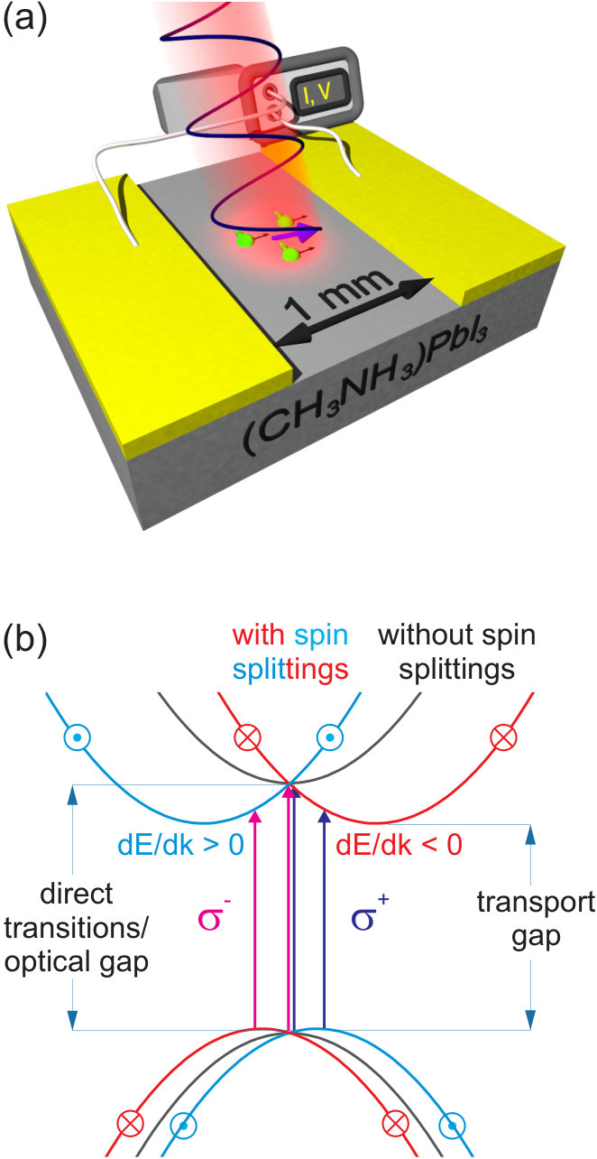 Figure 1
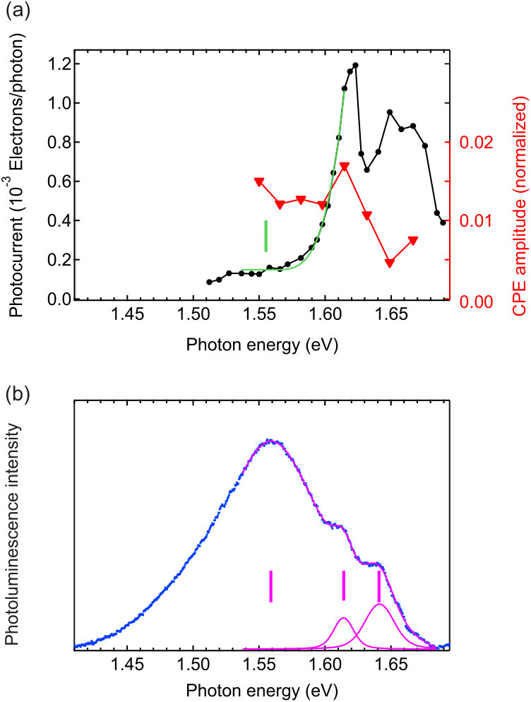 Figure 2
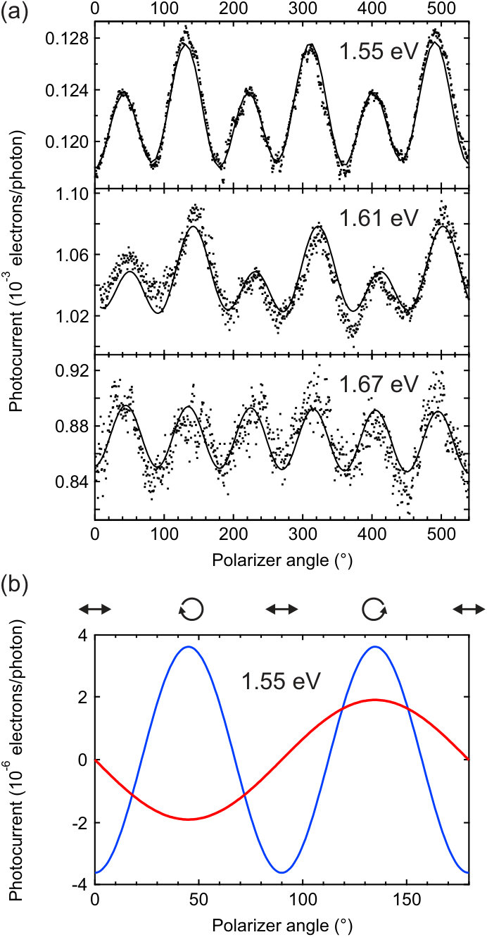 Figure 3
Peer Reviews
No public reviews on file for this paper yet. If you reviewed it on a platform where reviews are public (OpenReview, ICLR, NeurIPS, ICML), you can paste yours below so the community can read it here.
Videos
No videos yet. Explain this paper in a talk, walkthrough, or lecture? Add one.
Spin-split bands cause the indirect band gap of (CH3NH3)PbI3: Experimental evidence from circular photogalvanic effect
Daniel Niesner∗ present address: Columbia University, New York City. Email: [email protected] Lehrstuhl für Festkörperphysik, Friedrich-Alexander-Universität Erlangen-Nürnberg (FAU), Staudtstr. 7, 91058 Erlangen, Germany
Martin Hauck
Lehrstuhl für Angewandte Physik, Friedrich-Alexander-Universität Erlangen-Nürnberg (FAU), Staudtstr. 7, 91058 Erlangen, Germany
Shreetu Shrestha
Institute of Materials for Electronics and Energy Technology (I-MEET), Department of Materials Science and Engineering, Friedrich-Alexander-Universität Erlangen-Nürnberg (FAU), Martensstrasse 7, 91058 Erlangen, Germany
Ievgen Levchuk
Institute of Materials for Electronics and Energy Technology (I-MEET), Department of Materials Science and Engineering, Friedrich-Alexander-Universität Erlangen-Nürnberg (FAU), Martensstrasse 7, 91058 Erlangen, Germany
Gebhard J. Matt
Institute of Materials for Electronics and Energy Technology (I-MEET), Department of Materials Science and Engineering, Friedrich-Alexander-Universität Erlangen-Nürnberg (FAU), Martensstrasse 7, 91058 Erlangen, Germany
Andres Osvet
Institute of Materials for Electronics and Energy Technology (I-MEET), Department of Materials Science and Engineering, Friedrich-Alexander-Universität Erlangen-Nürnberg (FAU), Martensstrasse 7, 91058 Erlangen, Germany
Miroslaw Batentschuk
Institute of Materials for Electronics and Energy Technology (I-MEET), Department of Materials Science and Engineering, Friedrich-Alexander-Universität Erlangen-Nürnberg (FAU), Martensstrasse 7, 91058 Erlangen, Germany
Christoph Brabec
Institute of Materials for Electronics and Energy Technology (I-MEET), Department of Materials Science and Engineering, Friedrich-Alexander-Universität Erlangen-Nürnberg (FAU), Martensstrasse 7, 91058 Erlangen, Germany
Bavarian Center for Applied Energy Research (ZAE Bayern), Haberstrasse 2a, 91058 Erlangen, Germany
Heiko B. Weber
Lehrstuhl für Angewandte Physik, Friedrich-Alexander-Universität Erlangen-Nürnberg (FAU), Staudtstr. 7, 91058 Erlangen, Germany
Thomas Fauster
Lehrstuhl für Festkörperphysik, Friedrich-Alexander-Universität Erlangen-Nürnberg (FAU), Staudtstr. 7, 91058 Erlangen, Germany
Abstract
Long carrier lifetimes and diffusion lengths form the basis for the successful application of the organic-inorganic perovskite (CH3NH3)PbI3 in solar cells and lasers. The mechanism behind the long carrier lifetimes is still not completely understood. Spin-split bands and a resulting indirect band gap have been proposed by theory. Using near band-gap left-handed and right-handed circularly polarized light we induce photocurrents of opposite directions in a single-crystal (CH3NH3)PbI3 device at low temperature (4 K). The phenomenom is known as the circular photogalvanic effect and gives direct evidence for phototransport in spin-split bands. Simultaneous photoluminecence measurements show that the onset of the photocurrent is below the optical band gap. The results prove that an indirect band gap exists in (CH3NH3)PbI3 with broken inversion symmetry as a result of spin-splittings in the band structure. This information is essential for understanding the photophysical properties of organic-inorganic perovskites and finding lead-free alternatives. Furthermore, the optically driven spin currents in (CH3NH3)PbI3 make it a candidate material for spintronics applications.
Organic-inorganic perovskite semiconductors (OIPS) show remarkable potential for applications in highly efficient thin-film solar cells Yang2015 ; saliba2016 ; stranks2015 and nanolasers zhu2015 . Unusually long carrier lifetimes Bi2016 ; xu2016iodomethane and diffusion lengths stranks2013electron ; dong2015 form the basis of their exceptional performance in optoelectronic devices. Strong spin-orbit coupling due to the constituting heavy elements even2013 ; brivio2014 ; quarti2014 ; demchenko2016 and a resulting slightly indirect band gap have been proposed as origin of the observed long carrier lifetimes zheng2015 ; etienne2016 ; azarhoosh2016 . The direct-indirect character of the band gap of (CH3NH3)PbI3 was recently evidenced experimentally hutter2016 ; wang2016 . Direct experimental evidence for spin-orbit coupling as the origin of the indirect band gap, however, is still missing to the best of our knowledge.
To gain insight into the mechanism giving rise to the indirect gap of (CH3NH3)PbI3, we excite photocurrents with left-handed and right-handed circularly polarized light as illustrated in Fig. 1 (a). In the absence of spin-orbit coupling the direction of the excited photocurrent does not depend on the helicity of the incoming light. The spin structure of the electronic band structure causes differences in the optical transition matrix elements as illustrated in Fig. 1 (b). For opposite helicity of the light the group velocity of carriers is reversed and spin-polarized currents of opposite direction are induced belinicher1978 ; ganichev2014 . They enhance or reduce the overall photocurrent, respectively. The effect is known as the circular photogalvanic effect. It has been observed experimentally in GaAs/AlGaAs quantum well structures lechner2011 , in wurtzite semiconductors such as ZnO zhang2010 and GaN Weber2005 , in transition-metal dichalcogenides yuan2014 , and in the topological insulator Bi2Se3 mciver2012 . A circular photogalvanic effect of measurable magnitude has been predicted li2016circular for (CH3NH3)PbI3. Previously, circular dichroism has been found in optical giovanni2015 and electron spectroscopy niesner2016 experiments on OIPS. A circular photogalvanic effect is hence expected if coherent spin transport takes place on a length scale large enough for spin-polarized currents to be driven through a device.
Results of polarization-dependent photocurrent measurements performed on single-crystal (CH3NH3)PbI3 are shown in Fig. 2 (a) for different excitation photon energies. The sample temperature is 4 K. To control the polarization of the incident light a zero-order /4 plate is introduced in the excitation pathway. The polarizing waveplate is rotated while the photocurrent is measured. The angle of the /4 plate is given along the horizontal axis in Fig. 2 (a). At all wavelengths, a variation of the photocurrent is observed due to changing contributions of and -polarized light fields to the excitation. This signal has a periodicity of 90∘ in the angle of the waveplate. At an angle of () the light is -polarized and the photocurrent has a minimum. Local maxima occur at 45∘ (135∘), where the light is circularly polarized and the component of -polarized light is the largest. The variations may result from differences in reflectivity at the surface of the OIPS due to changing contributions of and -polarized light, from anisotropies in absorption along the crystalline directions associated with and polarization, and from a linear photogalvanic effect Ganichev2003 . Since differences in the photocurrents excited with -polarized light and circularly polarized light with -components can occur in any material and their interpretation is complex, they will not be in the focus of our discussion. However, it is worth noting that a linear photogalvanic effect necessarily goes hand in hand with the circular photogalvanic effect Ganichev2003 ; mciver2012 .
An additional modulation of the photocurrent induced by the light polarization is clearly observed upon excitation at 1.55 eV and 1.61 eV photon energy. This signal has a periodicity of 180∘ in the angle of the waveplate, resulting in different photocurrents at and . As these angles correspond to left-handed and right-handed circularly polarized light, the differences represent the circular photogalvanic effect. To extract the contribution of the circular photogalvanic effect to the photocurrent, we fit the data with a sum of two cosine functions. The two components are shown individually in Fig. 2 (b). The effect of linear polarization is given by the blue curve. The signal arising from the circular photogalvanic effect, indicated by the red curve, is phase-shifted by 90∘. Its contribution to the photocurrent vanishes whenever the light is linearly polarized (). For left-handed (45∘) and right-handed (135∘) circular polarization, in contrast, it switches sign. The reversal of the photocurrents as the helicity of the excitation light is switched is characteristic for materials with spin-split band structures Weber2005 ; zhang2010 ; lechner2011 ; mciver2012 ; yuan2014 . It implies that spin currents are driven by photoexcitation with circularly polarized light, as indicated in Fig. 1 (b). Light of different helicity couples to opposite branches of the spin-split band structure in -space. Since the opposite branches do not only carry electrons of opposite spin orientation, but also of reversed group velocity d/d, spin-polarized currents are induced along opposite directions. We observe a modification of the overall photocurrent by%. The amplitude of the circular photogalvanic effect relative to the average photocurrent is given by red symbols in Fig. 3 (a).
The photocurrent (normalized to electrons/photon) is shown as black dots connected by lines to guide the eye in Fig. 3(a). The onset of the photocurrent is well described by a fourth-power dependence on energy starting at eV. The large exponent can be understood as the result of an indirect band gap in combination with a low density of states of OIPS at the band edges endres2016 ; niesner2016 . A small current flows for photon energies below the onset because of the applied bias voltage. Note that the circular photogalvanic effect sets in right at the onset of the photocurrent. The photocurrent reaches its maximum at 1.62 eV photon energy which may be taken as an estimate for the direct band gap. This results in a difference between the direct and indirect gap of meV in agreement with literature hutter2016 ; wang2016 ; savenije2014 . The circular photogalvanic effect proves that the spin-orbit coupling of the Rashba effect is responsible for the indirect band gap in (CH3NH3)PbI3.
In order to corroborate the assignment of the direct band gap we performed in situ photoluminescence (PL) measurements on the sample at 4 K. A comparison of photocurrent excitation and PL spectra is given in Fig. 3. The low-temperature PL spectrum of (CH3NH3)PbI3 consists of a high-energy emission feature at eV, a second peak at eV, and broad low-energy continuum emission with a maximum at eV, in agreement with previous reports dar2016 ; diab2016 ; wu2015 ; galkowski2016a . The positions of the maxima are indicated by magenta tick marks in Fig. 3(b). Following the literature diab2016 , we assign the highest-energy peak at 1.64 eV to the optical band gap of orthorhombic (CH3NH3)PbI3. The value matches the optical band gap found from magneto-absorption measurements miyata2015 . Emission and absorption at lower photon energies have been attributed to excitons localized at defects wu2015 ; diab2016 and to coexisting structural phases galkowski2016a ; dar2016 . The assignment of optical transitions to bound or free excitons is difficult based on optical spectroscopy alone. Connecting the PL spectroscopy to the transport measurements at low temperature, we find that currents are generated with photon energies as low as 1.56 eV, demonstrating that free excitons are excited at these photon energies. We attribute the photocurrent to tetragonal phuong2016 ; galkowski2016a and low-symmetry orthorhombic dar2016 domains coexisting with the low-temperature, inversion-symmetric orthorhombic phase. The photocurrent has a maximum at eV which coincides with the second PL emission peak, indicating an allowed optical transition. We assign the maximum to the direct gap of the tetragonal and low-symmetry orthorhombic domains, in good agreement with the value of 1.61 eV found from magneto-absorption on tetragonal (CH3NH3)PbI3 miyata2015 ; galkowski2016 . The photocurrent drops by 40% as the photon energy exceeds the optical gap of 1.64 eV of orthorhombic (CH3NH3)PbI3. A smaller photocurrent in orthorhombic (CH3NH3)PbI3 than in the tetragonal phase has been reported before and assigned to less efficient generation of free excitons hutter2016 . Note that the amplitude of the circular photogalvanic effect also drops in the energy range when the inversion symmetric low-temperature orthorhombic phase contributes to the photocurrent.
The observed circular photogalvanic effect unambiguously identifies spin splittings in the band structure as the origin of the indirect gap. A slightly indirect band gap by 47 meV was reported for tetragonal (CH3NH3)PbI3 resulting in an enhanced lifetime of photoexcited carriers as compared to the direct band-gap orthorhombic phase hutter2016 . The lifetime enhancement was found to be absent in the low-temperature orthorhombic phase. While calculations point towards Rashba and Dresselhaus type spin splittings as the origin of the slightly indirect gap even2013 ; brivio2014 ; quarti2014 ; demchenko2016 ; wang2016 , experimental evidence for this interpretation is, to the best of our knowledge, lacking. Requirements for spin splittings are spin-orbit coupling and absence of inversion symmetry. It is worth noting that Rashba and Dresselhaus spin splittings are caused by the local environment of the atoms in the unit cell rather than by the average, long-range symmetry of the crystal zhang2014 . A Rashba-type spin-split band structure was found in the valence band at the surface of related (CH3NH3)PbBr3 perovskite using angle-resolved photoelectron spectroscopy niesner2016 . Surfaces break inversion symmetry inherently and enhance Rashba splitting. Observation of the circular photogalvanic effect demonstrates that spin-splittings occur in the bulk of (CH3NH3)PbI3 on a length scale relevant for carrier transport. We find a stronger effect at low photon energies than for higher ones. The corresponding transitions can be assigned to tetragonal and low-symmetry orthorhombic domains ( eV) and to the inversion symmetric low-temperature orthorhombic phase ( eV), respectively. For the latter, a prominent photogalvanic effect is not expected. The former, in contrast, has a locally broken inversion symmetry at all temperatures druzbicki2016 ; beecher2016 . The spin splittings in the band structure observed here at 4 K are hence expected to persist for temperatures up to room temperature, as implied also by the strong circular dichroism found in optical spectroscopy at room temperature giovanni2015 .
The observed difference between the optical and the transport gap of meV of tetragonal (CH3NH3)PbI3 is large enough to pose an energetic barrier for electron-hole-pair recombination even at room temperature. Activation energies of 75 meV savenije2014 and 47 meV hutter2016 for radiative recombination were reported previously, in good agreement with our results. Calculations find a value of 75 meV as a result of spin-splittings in the band structure of (CH3NH3)PbI3 azarhoosh2016 . They predict an increasing splitting with increasing temperature, in agreement with optical spectroscopic results obtained from related (CH3NH3)PbBr3 single crystals niesner2016optical .
Our results clarify the mechanism behind the indirect character of the band gap of (CH3NH3)PbI3. This helps to understand the excellent performance of OIPS in optoelectronic devices and provides a design rule for less toxic alternatives to (CH3NH3)PbI3. Lifetime enhancements by a factor of 10 to 350 have been predicted as the result of Rashba-type spin splitting restricting optical transitions zheng2015 ; etienne2016 ; azarhoosh2016 , making it an essential ingredient to the observed long carrier diffusion lengths. hutter2016
Spin splittings of this magnitude do not only enhance carrier lifetimes. They also allow to optically drive spin currents kepenekian2015 ; Li2016 ; zhang2017 in the system. The spin splitting of meV is similar to the strongest ones found in known bulk Rashba systems, such as BiTeX (X Cl landolt2013 , Br ogawa2014 , I Ishizaka2011 ) and GeTe(111) liebmann2016 . In contrast to these materials, (CH3NH3)PbI3 has a band gap in the near-infrared range making it a candidate material for opto-spintronics applications Li2016 . Additional applications become possible if structures with a switchable ferroelectric polarization can be grown kim2014 ; leppert2016 , as they have been found at the surface of (CH3NH3)PbI3 kutes2014 , where the Rashba splitting in organic-inorganic perovskite is further enhanced niesner2016 .
We find a measurable circular photogalvanic effect of % in rather large devices with a channel width of 1 mm. Significant spin currents can be expected when device dimensions are reduced to the spin transport length. From magneto-transport and magneto-optical experiments, a spin-lattice relaxation time of 200 ps was estimated for spin-cast (CH3NH3)PbI3 thin films zhang2015magnet . Carrier diffusion coefficients in (CH3NH3)PbI3 thin films are around cm stranks2013electron ; guo2015spatial , translating into a spin diffusion length nm. The carrier diffusion constant in single crystals is larger than in thin films by a factor of shi2015 ; dong2015 ; guo2015spatial , and also the spin relaxation time can be expected to be enhanced. Spin diffusion lengths of hundreds of nanometers may hence be achieved in OIPC single crystals.
Acknowledgements
I. L., A. O., S. S., M. B., and C. J. B. gratefully acknowledge financial support from the Soltech Initiative, the Excellence Cluster ”Engineering of Advanced Materials” (EAM) granted to the University Erlangen-Nuremberg, and from the Energiecampus Nürnberg. Funding from the Emerging Fields initiative ”Singlet Fission” supported by Friedrich-Alexander-Universität Erlangen-Nürnberg is gratefully acknowledged by D. N., M. W., and T. F.
Methods
Device fabrication.
(CH3NH3)PbI3 single crystals were grown by the seed-solution growth method following the procedure described in Ref. zhou2016giant . Crystals were prepared and kept under N2 atmosphere before they got contacted with 40 nm of gold at a spacing of 1 mm. Contacts are aligned with the macroscopic facets of the crystals. The crystals are mounted under ambient conditions (exposure for h) in a vacuum cryostat. Immediately after pumping the cryostat, crystals are cooled to 4 K. Keeping the crystals in vacuum at room temperature for extended periods of time ( h) results in changes in the spectra, whereas no changes are observed for the cooled crystals under prolonged (4 h) illumination with laser light, see Fig. S1 in Supplementary Information. We demonstrated that methylamine desorbs from (CH3NH3)PbBr3 in vacuum just above room temperature niesner2016 and speculatively assign the degradation of (CH3NH3)PbI3 to the same mechanism.
Photocurrent and photoluminescence measurements.
Photocurrents are excited with a Ti:Sa laser in cw mode. Laser powers are around 3 mW with a Gaussian spot radius of 0.3 mm. The voltage applied to the device is swept between V and V to avoid slow changes gottesman2014extremely ; gottesman2015photoinduced in the structure of (CH3NH3)PbI3. No hysteresis is observed in the I(V) sweeps, see Fig. S2 in Supplementary Information. The data are shown for a small bias voltage (0.25 V). Results presented here are independent of the applied bias voltage for V except for the amplitude of the measured photocurrents. Photocurrents are normalized to the number of incident photons to account for variations in the laser power at different photon energies. The photocurrent increases linearly with excitation density as shown in Fig. S3 in Supplementary Information.
For photoluminescence experiments the channel of the (CH3NH3)PbI3 device was optically excited with a 532 nm cw laser between photocurrent measurementss. The PL spectra were recorded using an Ocean Optics HR 4000 spectrometer. A dielectric long pass filter (550 nm) was used to suppress scattered light from the illuminated surface from which the PL was collected.
The reference list from the paper itself. Each links out to its DOI / PubMed record.
- 1(1) Yang, W. S. et al. High-performance photovoltaic perovskite layers fabricated through intramolecular exchange. Science 348 , 1234–1237 (2015).
- 2(2) Saliba, M. et al. A molecularly engineered hole-transporting material for efficient perovskite solar cells. Nat. Energy 1 , 15017 (2016).
- 3(3) Stranks, S. D. & Snaith, H. J. Metal-halide perovskites for photovoltaic and light-emitting devices. Nat. Nanotechnol. 10 , 391–402 (2015).
- 4(4) Zhu, H. et al. Lead halide perovskite nanowire lasers with low lasing thresholds and high quality factors. Nat. Mater. 14 , 636–642 (2015).
- 5(5) Bi, Y. et al. Charge Carrier Lifetimes Exceeding 15 μ 𝜇 \mu s in Methylammonium Lead Iodide Single Crystals. J. Phys. Chem. Lett. 7 , 923 (2016).
- 6(6) Xu, W. et al. Iodomethane-Mediated Organometal Halide Perovskite with Record Photoluminescence Lifetime. ACS Appl. Mater. Interfaces 8 , 23181–23189 (2016).
- 7(7) Stranks, S. D. et al. Electron-hole diffusion lengths exceeding 1 micrometer in an organometal trihalide perovskite absorber. Science 342 , 341–344 (2013).
- 8(8) Dong, Q. et al. Electron-hole diffusion lengths > 175 μ absent 175 𝜇 >175~{}\mu m in solution-grown CH 3 NH 3 Pb I 3 single crystals. Science 347 , 967 (2015).