Lateral p-n Junction in an Inverted InAs/GaSb Double Quantum Well
Matija Karalic, Christopher Mittag, Thomas Tschirky, Werner, Wegscheider, Klaus Ensslin, Thomas Ihn

TL;DR
This study investigates a lateral p-n junction in an inverted InAs/GaSb double quantum well, revealing diode-like behavior at zero magnetic field and complex edge state interactions under magnetic fields, advancing topological state research.
Contribution
It demonstrates the transport properties of a lateral p-n junction in InAs/GaSb quantum wells and explores edge state interactions in the quantum Hall regime, providing insights for topological state transitions.
Findings
Diodelike behavior at zero magnetic field.
Edge state mixing and full equilibration at high magnetic fields.
Potential for probing topological quantum phase transitions.
Abstract
We present transport measurements on a lateral p-n junction in an inverted InAs/GaSb double quantum well at zero and nonzero perpendicular magnetic fields. At a zero magnetic field, the junction exhibits diodelike behavior in accordance with the presence of a hybridization gap. With an increasing magnetic field, we explore the quantum Hall regime where spin-polarized edge states with the same chirality are either reflected or transmitted at the junction, whereas those of opposite chirality undergo a mixing process, leading to full equilibration along the width of the junction independent of spin. These results lay the foundations for using p-n junctions in InAs/GaSb double quantum wells to probe the transition between the topological quantum spin Hall and quantum Hall states.
Click any figure to enlarge with its caption.
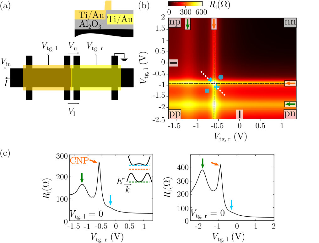 Figure 1
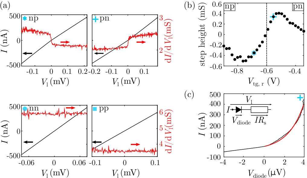 Figure 1
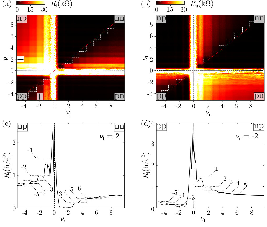 Figure 2
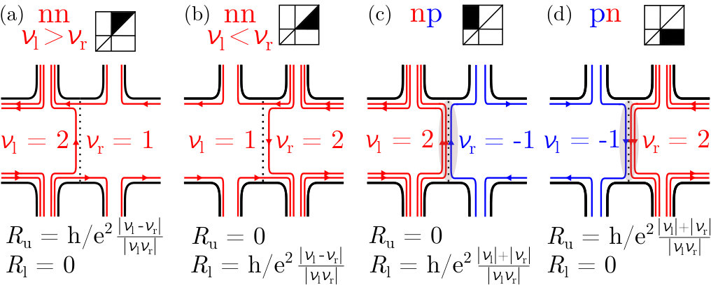 Figure 3
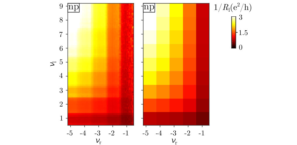 Figure 4
Peer Reviews
No public reviews on file for this paper yet. If you reviewed it on a platform where reviews are public (OpenReview, ICLR, NeurIPS, ICML), you can paste yours below so the community can read it here.
Videos
No videos yet. Explain this paper in a talk, walkthrough, or lecture? Add one.
Lateral p-n Junction in an Inverted InAs/GaSb Double Quantum Well
Matija Karalic
Solid State Physics Laboratory, ETH Zurich, 8093 Zurich, Switzerland
Christopher Mittag
Solid State Physics Laboratory, ETH Zurich, 8093 Zurich, Switzerland
Thomas Tschirky
Solid State Physics Laboratory, ETH Zurich, 8093 Zurich, Switzerland
Werner Wegscheider
Solid State Physics Laboratory, ETH Zurich, 8093 Zurich, Switzerland
Klaus Ensslin
Solid State Physics Laboratory, ETH Zurich, 8093 Zurich, Switzerland
Thomas Ihn
Solid State Physics Laboratory, ETH Zurich, 8093 Zurich, Switzerland
Abstract
We present transport measurements on a lateral p-n junction in an inverted InAs/GaSb double quantum well at zero and nonzero perpendicular magnetic fields. At a zero magnetic field, the junction exhibits diodelike behavior in accordance with the presence of a hybridization gap. With an increasing magnetic field, we explore the quantum Hall regime where spin-polarized edge states with the same chirality are either reflected or transmitted at the junction, whereas those of opposite chirality undergo a mixing process, leading to full equilibration along the width of the junction independent of spin. These results lay the foundations for using p-n junctions in InAs/GaSb double quantum wells to probe the transition between the topological quantum spin Hall and quantum Hall states.
Diodes based on p-n junctions are one of the basic building blocks of electronic systems, with a multitude of applications including rectification, switching, signal generation and amplification, light emission, as well as photovoltaics. Advances in materials research in recent years have produced p-n junctions in a variety of novel systems such as graphene Huard et al. (2007); Williams et al. (2007) and transition-metal dichalcogenides Jariwala et al. (2013); Lee et al. (2014), an emerging class of two-dimensional semiconductors Wang et al. (2012); Jariwala et al. (2014). Beyond practical accomplishments such as downscaling, these junctions also allow us to gain new insights into fundamental physical phenomena, for example, how electron and hole edge states interact with each other in the quantum Hall (QH) regime Williams et al. (2007); Özyilmaz et al. (2007).
Here, we study the formation of a lateral p-n junction using local top gating in an inverted InAs/GaSb double quantum well (QW) heterostructure, a semiconductor system that naturally hosts both electrons and holes that are spatially separated in the vertical (growth) direction. Depending on the thicknesses of the InAs and GaSb layers, it intrinsically possesses inverted or noninverted band alignment. Furthermore, the band alignment is affected by both electric and magnetic fields, allowing for continuous tuning between the two phases Naveh and Laikhtman (1995); Qu et al. (2015); Suzuki et al. (2015). In the inverted phase, coupling between the bands leads to the opening of a hybridization gap Lakrimi et al. (1997); Yang et al. (1997); Cooper et al. (1998) hosting topologically protected helical edge states, making InAs/GaSb double QWs a two-dimensional topological insulator (TI) or quantum spin Hall (QSH) insulator Liu et al. (2008); Knez et al. (2011); Suzuki et al. (2013); Knez et al. (2014); Du et al. (2015). Apart from the TI properties of the system, it is also of more general interest due to its complex band structure Altarelli (1983); de-Leon et al. (1999), strong spin-orbit interaction (SOI) Li et al. (2009); Karalic et al. (2016); Nichele et al. (2017), and optical properties Smith and Mailhiot (1987).
A pair of overlapping top gates enables us to independently control carrier type and density in two adjacent parts of the sample at a zero magnetic field and in the QH regime. At a zero field and when the two parts are populated by charge carriers of opposite polarity, the electrons and holes situated in their respective QWs are separated in energy by the hybridization gap responsible for the QSH insulator properties of these QWs. This gap allows the junction to function as a diode in the appropriate regimes, which is a novel signature of the gap that has not been experimentally explored. In the QH regime, we detect full equilibration along the p-n junction between counterpropagating spin-polarized electron and hole edge states. Fractional plateaus occurring due to equilibration are seen in the junction resistance over many filling factors, consistent with scattering between edge states with different spin polarizations, and attest to the versatility of our junction. These findings open up possibilities for using p-n junctions to investigate QSH and QH edge state dynamics and their interplay Gusev et al. (2013); Calvo et al. (2017) in InAs/GaSb double QWs, in particular because the QSH effect has been reported to persist up to high magnetic fields where time-reversal symmetry is broken Du et al. (2015).
Measurements were performed on patterned heterostructures comprising an nm GaSb QW and a nm InAs QW grown on a GaSb substrate. The wafer structure is identical to the one in Ref. 22. We fabricated a lateral p-n junction by chemical wet etching and subsequent atomic layer deposition of a nm Al2O3 layer, followed by evaporation of Ti/Au for the first top gate. A further Al2O3 layer was deposited to isolate the second top gate from the first. The top gates overlap partially to guarantee the formation of a junction, and the bottom gate completely screens the upper gate in the region of overlap [see the inset of Fig. 1(a)]. Ohmic contacts were made by etching through the oxide stack, then selectively down to the InAs QW and depositing Ti/Au without annealing. All experiments were conducted in a dilution refrigerator at a base temperature of mK using low-frequency lock-in techniques with constant ac voltage bias, unless stated otherwise.
Figure 1(a) schematically depicts the sample layout. The separation of the inner contact pairs between which the junction is formed is around . A current flowing across the junction results in a voltage measured along the upper and lower edges of the sample, labeled and , respectively. The junction resistance at a zero magnetic field behaves as shown in the color map in Fig. 1(b) as a function of the two top gate voltages and . We identify four unique regions in the phase diagram corresponding to different majority charge carrier configurations under the gates (pp, pn, nn, and np), as indicated by the dashed lines. The observed resistance is mainly the series addition of p and n region resistances. Two line cuts [see Fig. 1(c)], at and , reveal the known sharp resistance peak coinciding with the charge neutrality point (CNP), which occurs as the Fermi energy passes through the hybridization gap. Apart from the CNP peak, we find another prominent peak when the Fermi energy is close to the bottom of the conduction band, as illustrated in the inset, as well as a here barely noticeable shoulder, presumably due to van Hove singularities in the density of states occurring at Karalic et al. (2016).
When the sample is tuned into the pn and np regions it behaves as a diode, as revealed by taking - traces at various points in the phase diagram in Fig. 2(a). Under forward bias, the junction carries more current than under reverse bias, resulting in a step in the differential conductance around zero voltage. When crossing from the pn into the np region, forward and reverse bias directions are interchanged as expected. The step width in bias voltage increases monotonically with increasing temperature. The diodelike behavior of the junction gradually disappears deeper into the pn and np regions with increasing charge carrier densities, and the - dependence becomes Ohmic, as is the case everywhere in the pp and nn regions. Figure 2(b) shows the step height in the differential conductance around zero voltage along the diagonal dotted line in Fig. 1(b), exhibiting the sign change around the CNP and the aforementioned gradual disappearance of the diode behavior.
The p-n junction can be modeled as an ideal diode in series with a resistor which is the total resistance of the regions between the voltage probes outside the depletion region [inset of Fig. 2(c)], and the diode characteristic - curve can be extracted from the measurement, Fig. 2(c). The diode voltage is given by , where we take to be the resistance that limits the current under sufficiently large forward bias ( is the flat part in for large forward bias). The - curve obtained in this manner is approximately exponential, as seen in Fig. 2(c).
We speculate that the reason behind the disappearance of the diode behavior with increasing density is the decreasing depletion region width, so that tunneling progressively degrades the diode properties.
Note that when the sample is in the pn and np regions, the Fermi energy inevitably passes through the hybridization gap when crossing the junction, and is predicted to intersect the topologically protected QSH states, leading to helical edge transport along the depletion region at the edges of the etched structure where the junction terminates and normal band ordering is restored. Unfortunately, in our heterostructure the bulk is not insulating enough to study this phenomenon in a detailed fashion. However, the existence of a gap is a necessary prerequisite for the observed diode properties of the junction. Therefore, we believe that the diode behavior is a signature of the hybridization gap that has not been reported in the literature so far.
Now, we turn to the properties of the p-n junction in a perpendicular magnetic field such that the system is in the QH regime. We focus on the results obtained for T, which is sufficient to fully spin split the Landau levels (LLs). Measurements at other magnetic fields in the QH regime yield similar results.
Figures 3(a) and 3(b) depict color maps of the junction resistances and for T as a function of and , the filling factors under the left and right gates, respectively. We label electron LLs with positive integers and hole LLs with negative integers. Again, we discern the four quadrants discussed earlier separated by resistance maxima, as indicated by the dashed lines. The positions in gate voltage of these resistance maxima around are shifted towards more negative gate voltages compared to their positions at , which may be a signature of helical edge transport close to due to the inverted band structure of our system, as recently postulated in Ref. 26.
Apart from the four quadrants, the pp and nn regions can be additionally subdivided into two triangles, in one of which the resistance vanishes. In the other triangle, a staircaselike pattern emerges, as implied by the dashed-dotted lines. The triangles are separated by the dotted line along which the densities under the gates are equal, . This line is simultaneously the mirror symmetry line mapping to and vice versa.
is quantized in the np region, exhibiting plateaus. The same holds true in the pp and nn regions when (lower triangles). In contrast, vanishes in the pn region as well as in the pp and nn regions when (upper triangles). behaves as , but mirrored with respect to the line.
In the pp and nn regions, the observed plateaus can be understood in an edge state picture invoking perfect reflection and transmission at the junction Haug et al. (1988); Washburn et al. (1988), as exemplarily elucidated in Figs. 4(a) and 4(b). The additional edge states in the region of higher filling factor are perfectly reflected at the junction, whereas the other are perfectly transmitted. Depending on the chirality of the edge states, this leads to a vanishing resistance or because the corresponding voltage contacts are shorted by the transmitted edge states common to both sides of the junction. The resistance on the opposite edge of the sample is then quantized because it involves at least one reflected edge state present on one junction side only. The expected resistance quantization is given by Büttiker et al. (1985); Büttiker (1986); Haug et al. (1988); Washburn et al. (1988)
[TABLE]
and exchange roles when crossing the line, as seen in Figs. 3(a) and 3(b).
In the pn and np regions, in the absence of edge state mixing no current should flow through the sample and , are expected to diverge. Instead, here we find quantized junction resistances that can be explained by complete mode mixing, similarly to experiments on p-n junctions in graphene Williams et al. (2007); Özyilmaz et al. (2007); Ki et al. (2010); Amet et al. (2014). Referring to Figs. 4(c) and 4(d), we note that electron and hole edge states copropagate along the junction due to their opposite chiralities. If scattering processes lead to full equilibration of the electrochemical potentials of these edge states while they traverse the width of the junction, we expect to measure a resistance equal to zero between the voltage contacts on the far sample edge, which the edge states reach after having mixed. The resistance on the opposite edge (prior to mixing) should then follow Abanin and Levitov (2007)
[TABLE]
Figures 3(c) and 3(d) show line cuts of Fig. 3(a) at and . The dotted lines indicate the expected positions of fractional resistance plateaus, calculated using Eq. (1) in the pp and nn regions and Eq. (2) in the pn and np regions. Based on the coincidence of the measured plateaus and their expected positions, we conclude that the spin-polarized edge states indeed mix completely independent of their spin, which is not the case in graphene p-n junctions where equilibration is spin selective Amet et al. (2014).
Figure 5 presents a full comparison between experiment (left panel) and theory (right panel) for the conductance quantization of in the np region of Fig. 3(a). The color scale is identical for both panels. The right panel is generated according to Eq. (2). The agreement between experiment and theory is excellent and spans many filling factors. The only exception is if either or , where the resistance can be up to lower than expected. Experimentally, the gap is most sensitive to temperature and applied bias. We think that this fragility of the gap is the reason for the decreased plateau resistance.
We believe that the fact that edge states with different spin polarization undergo complete mixing occurs due to the known strong SOI in InAs/GaSb double QWs, which causes the particle’s spin to not be exclusively determined by the external magnetic field, but also by internal, SOI induced fields, facilitating mixing between edge states independent of their spin Müller et al. (1992). If only edge states of identical spin were to mix, Eq. (2) would no longer be valid. Instead, it would be replaced by with , where and are given by Eq. (2), but only counting those edge states with spin up or spin down in each case.
In contrast to edge state mixing experiments in GaAs QWs Haug et al. (1988); Washburn et al. (1988) or graphene Williams et al. (2007); Özyilmaz et al. (2007); Ki et al. (2010); Amet et al. (2014), our system is made up of two distinct constituent parts, and the electron and hole LL spectra differ vastly: Kim et al. (1988). The electron and hole states are also spatially separated in the growth direction of the heterostructure. The situation is more complex in the vicinity of the CNP where the effects of hybridization are most pronounced.
In conclusion, we have investigated the properties of a lateral p-n junction in an inverted InAs/GaSb double QW. At a zero magnetic field, the junction shows diodelike behavior in the pn and np regions, which we link to the presence of the hybridization gap. In the QH regime, measurements of the junction resistance on the upper and lower edges of the sample reveal that edge states of the same chirality (pp, nn regions) undergo perfect transmission and reflection, whereas those of opposite chirality (pn, np regions) mix, leading to full equilibration of electrochemical potentials. The mixing process does not discriminate between the spin polarization or the host material of the involved edge states, demonstrating it is a robust phenomenon. p-n junctions in InAs/GaSb double QWs are useful for studying the interplay of QSH and QH edge states in a controlled manner. Additionally, p-n junctions may serve as basic building blocks in more advanced quantum devices based on TIs.
Acknowledgements.
The authors acknowledge the support of the ETH FIRST laboratory and the financial support of the Swiss Science Foundation (Schweizerischer Nationalfonds, NCCR QSIT).
The reference list from the paper itself. Each links out to its DOI / PubMed record.
- 1Huard et al. (2007) B. Huard, J. A. Sulpizio, N. Stander, K. Todd, B. Yang, and D. Goldhaber-Gordon, Phys. Rev. Lett. 98 , 236803 (2007) . · doi ↗
- 2Williams et al. (2007) J. R. Williams, L. Di Carlo, and C. M. Marcus, Science 317 , 638 (2007) . · doi ↗
- 3Jariwala et al. (2013) D. Jariwala, V. K. Sangwan, C.-C. Wu, P. L. Prabhumirashi, M. L. Geier, T. J. Marks, L. J. Lauhon, and M. C. Hersam, Proc. Natl. Acad. Sci. U.S.A. 110 , 18076 (2013) . · doi ↗
- 4Lee et al. (2014) C.-H. Lee, G.-H. Lee, A. M. van der Zande, W. Chen, Y. Li, M. Han, X. Cui, G. Arefe, C. Nuckolls, T. F. Heinz, J. Guo, J. Hone, and P. Kim, Nat. Nanotechnol. 9 , 676 (2014) . · doi ↗
- 5Wang et al. (2012) Q. H. Wang, K. Kalantar-Zadeh, A. Kis, J. N. Coleman, and M. S. Strano, Nat. Nanotechnol. 7 , 699 (2012) . · doi ↗
- 6Jariwala et al. (2014) D. Jariwala, V. K. Sangwan, L. J. Lauhon, T. J. Marks, and M. C. Hersam, ACS Nano 8 , 1102 (2014) . · doi ↗
- 7Özyilmaz et al. (2007) B. Özyilmaz, P. Jarillo-Herrero, D. Efetov, D. A. Abanin, L. S. Levitov, and P. Kim, Phys. Rev. Lett. 99 , 166804 (2007) . · doi ↗
- 8Naveh and Laikhtman (1995) Y. Naveh and B. Laikhtman, Appl. Phys. Lett. 66 , 1980 (1995) . · doi ↗