Enhanced Light-Matter Interaction in Graphene/h-BN van der Waals Heterostructures
Wahib Aggoune, Caterina Cocchi, Dmitrii Nabok, Karim Rezouali, Mohamed, Akli Belkhir, Claudia Draxl

TL;DR
This study demonstrates that graphene/h-BN heterostructures exhibit significantly enhanced and tunable light-matter interactions across a broad spectrum, enabling tailored optoelectronic properties through stacking arrangements.
Contribution
It provides a comprehensive ab initio analysis showing how stacking modulates excitations and enhances light absorption in graphene/h-BN heterostructures, revealing new design possibilities.
Findings
Broad spectral light absorption from near-infrared to UV
Distinct excitations for each spectral region
Stacking arrangement controls electron-hole distribution
Abstract
By investigating the optoelectronic properties of prototypical graphene/hexagonal boron nitride (h-BN) heterostructures, we demonstrate how a nanostructured combination of these materials can lead to a dramatic enhancement of light-matter interaction and give rise to unique excitations. In the framework of ab initio many-body perturbation theory, we show that such heterostructures absorb light over a broad frequency range, from the near-infrared to the ultraviolet (UV), and that each spectral region is characterized by a specific type of excitations. Delocalized electron-hole pairs in graphene dominate the low-energy part of the spectrum, while strongly bound electron-hole pairs in h-BN are preserved in the near-UV. Besides these features, characteristic of the pristine constituents, charge-transfer excitations appear across the visible region. Remarkably, the spatial distribution of…
Click any figure to enlarge with its caption.
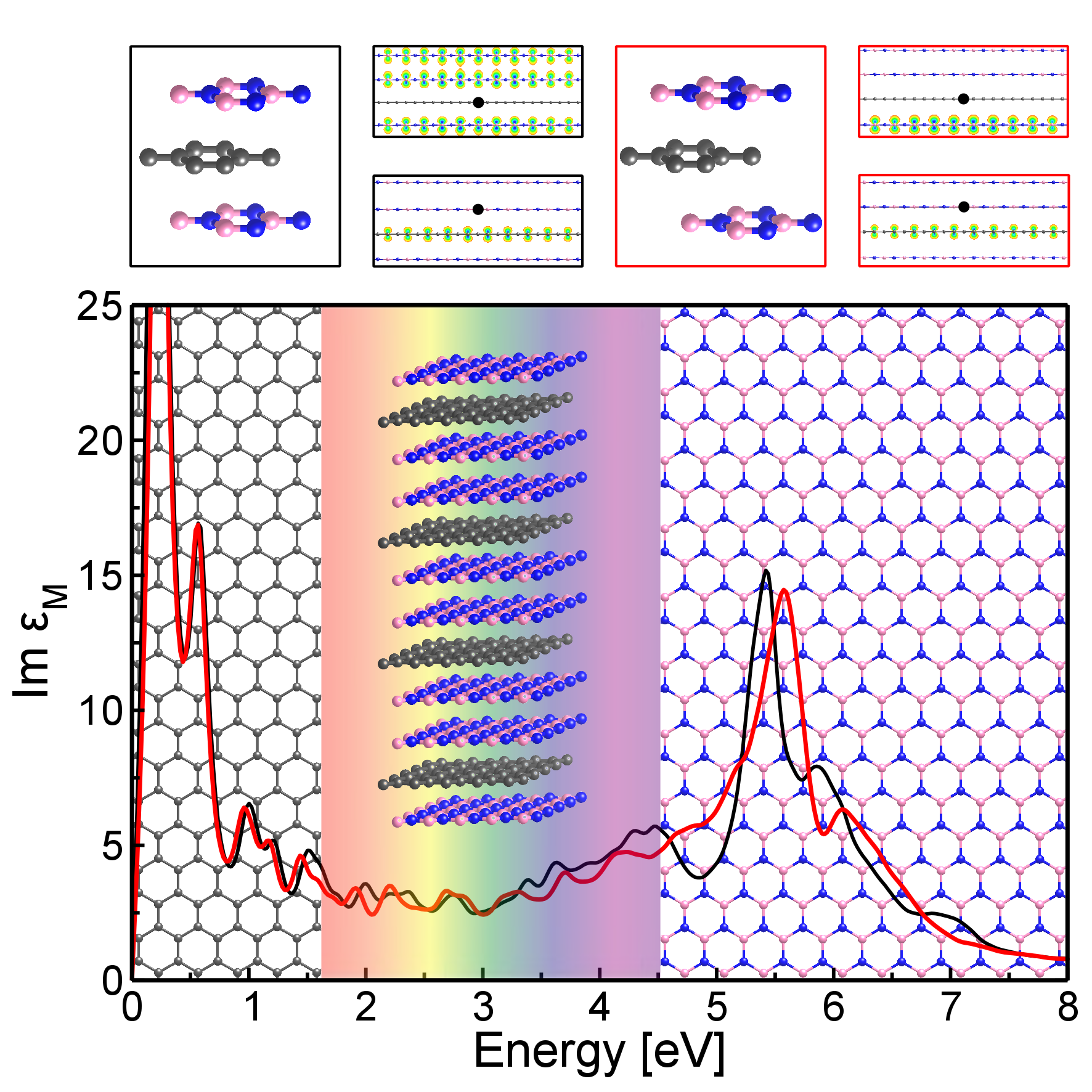 Figure 1
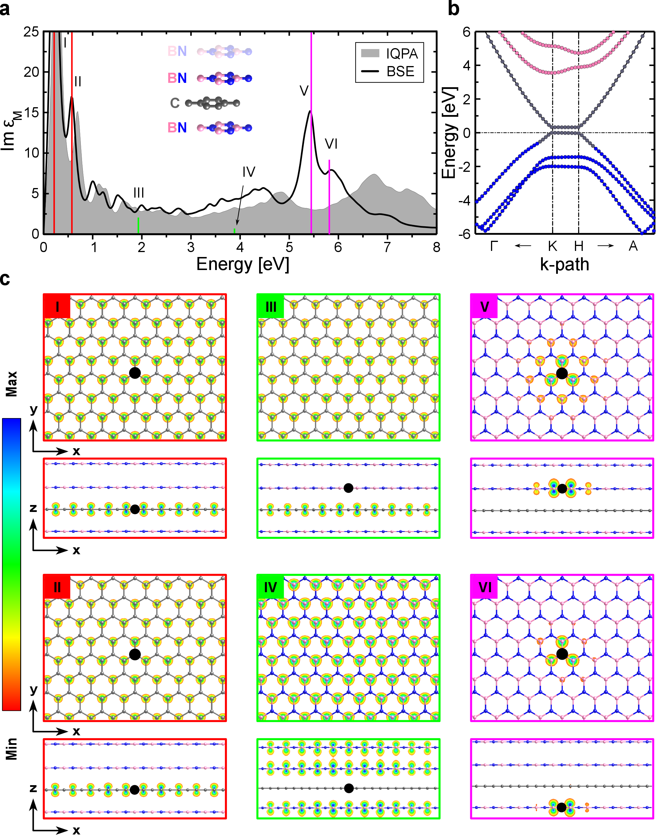 Figure 2
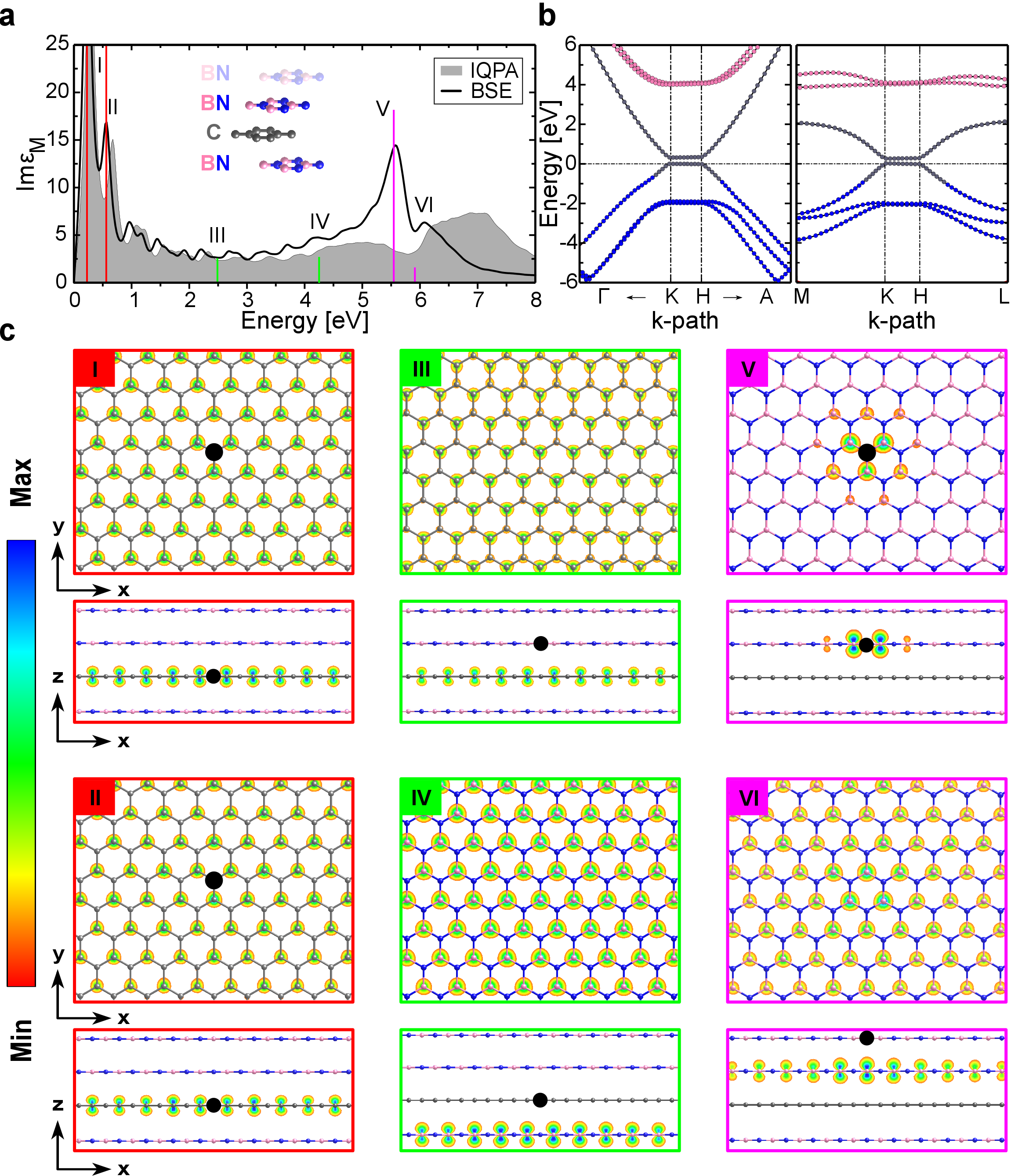 Figure 3
 Figure 4
Peer Reviews
No public reviews on file for this paper yet. If you reviewed it on a platform where reviews are public (OpenReview, ICLR, NeurIPS, ICML), you can paste yours below so the community can read it here.
Videos
No videos yet. Explain this paper in a talk, walkthrough, or lecture? Add one.
Enhanced Light-Matter Interaction in Graphene/h-BN van der Waals Heterostructures
Wahib Aggoune
Institut für Physik and IRIS Adlershof, Humboldt-Universität zu Berlin, 12489 Berlin, Germany
Caterina Cocchi
Institut für Physik and IRIS Adlershof, Humboldt-Universität zu Berlin, 12489 Berlin, Germany
Dmitrii Nabok
Institut für Physik and IRIS Adlershof, Humboldt-Universität zu Berlin, 12489 Berlin, Germany
Karim Rezouali
Laboratoire de Physique Théorique, Faculté des Sciences Exactes, Université de Bejaia, 06000 Bejaia, Algeria
Mohamed Akli Belkhir
Laboratoire de Physique Théorique, Faculté des Sciences Exactes, Université de Bejaia, 06000 Bejaia, Algeria
Claudia Draxl
Institut für Physik and IRIS Adlershof, Humboldt-Universität zu Berlin, 12489 Berlin, Germany
Abstract
By investigating the optoelectronic properties of prototypical graphene/hexagonal boron nitride (h-BN) heterostructures, we demonstrate how a nanostructured combination of these materials can lead to a dramatic enhancement of light-matter interaction and give rise to unique excitations. In the framework of ab initio many-body perturbation theory, we show that such heterostructures absorb light over a broad frequency range, from the near-infrared to the ultraviolet (UV), and that each spectral region is characterized by a specific type of excitations. Delocalized electron-hole pairs in graphene dominate the low-energy part of the spectrum, while strongly bound electron-hole pairs in h-BN are preserved in the near-UV. Besides these features, characteristic of the pristine constituents, charge-transfer excitations appear across the visible region. Remarkably, the spatial distribution of the electron and the hole can be selectively tuned by modulating the stacking arrangement of the individual building blocks. Our results open up unprecedented perspectives in view of designing van der Waals heterostructures with tailored optoelectronic features.
\alsoaffiliation
Laboratoire de Physique Théorique, Faculté des Sciences Exactes, Université de Bejaia, 06000 Bejaia, Algeria
\alsoaffiliationEuropean Theoretical Spectroscopic Facility (ETSF)
\alsoaffiliationEuropean Theoretical Spectroscopic Facility (ETSF)
\alsoaffiliationEuropean Theoretical Spectroscopic Facility (ETSF)
Graphical TOC Entry
Keywords: 2D materials, excitons, many-body perturbation theory, UV-vis spectra
Van der Waals (vdW) heterostructures are a new frontier of materials science 1. The possibility of stacking atomically-thin layers with nanoscale precision has opened unprecedented opportunities to create materials with customized characteristics. New properties can be accessed through a combination of the constituents, which maintain their intrinsic features 2, 3. This perspective is particularly appealing in the field of optoelectronics. The response of materials to electromagnetic radiation, consisting in a multitude of diversified phenomena, is extremely sensitive to their atomic structure and, consequently, to their electronic properties. Systems efficiently absorbing over a broad frequency range can be designed through an engineered stacking of single layers. Charge-transfer excitations, with the electron and the hole delocalized on different layers, can be created at the interface 4, 5, 6, 7, 8, 9. At the same time, the spatial separation of the electron-hole pairs can be enhanced through a systematic modulation of the structural properties 10, 11, 12.
Graphene and hexagonal boron nitride (h-BN) monolayers are ideal candidates to achieve this goal, as they exhibit a complementary behavior when interacting with light. The optical spectrum of graphene, a peculiar semi-metal 13, is dominated by a zero-energy resonance, while it is rather featureless in the visible region 14. Collective excitations, such as excitons and plasmons, occur only at ultraviolet (UV) frequencies 15, 16, 17, 18. On the other hand, h-BN is a large band-gap material transparent to visible light, which exhibits unique optical properties in the near-UV range 19, 20 related to the presence of strongly bound excitons 21, 22, 23. Combining these two materials to form a vdW heterostructure enables one to benefit from their individual characteristics and to access new features 24. The small mismatch between their lattices has already triggered a number of pioneering studies in this direction 25, 26, 27, 28, further boosted by the opportunity to exploit h-BN in view of opening a band gap in graphene 29, 30, 31. When interacting with light, graphene/h-BN vdW heterostructures are expected to show all their potential 32, as recently demonstrated also for plasmonic excitations 33, 34, 35.
In this work, we study the optoelectronic properties of prototypical periodic graphene/h-BN heterostructures. Through a detailed analysis of the spectra, enabled by a highly precise state-of-the-art ab initio many-body approach, we demonstrate that different types of excitations coexist in such a system, each of them dominating a well-defined frequency range. We focus on charge-transfer excitations that are created at the interface and show that a selective modulation of the stacking of h-BN layers with respect to each other and to graphene can tune the spatial distribution of the electron-hole (-) pairs. As such, our results pave the way for selectively enhancing light-matter interaction through nano-patterning.
To perform this study we consider a periodic heterostructure with a graphene sheet sandwiched between four h-BN layers. Such a system is modeled by a trilayer unit cell (h-BN/graphene/h-BN), infinitely replicated by means of periodic boundary conditions. In this configuration, each h-BN layer directly interacts with both graphene and another h-BN sheet. An important parameter is represented by the stacking arrangement of the layers in the in-plane directions. Here we focus on a structure where h-BN layers are displaced with respect to graphene such that the N atoms are located on hollow sites with respect to the hexagonal carbon lattice (Fig. 1a, inset). We refer to this configuration as the B-g-B stacking, where g stands for graphene, and B indicates the displacement of the h-BN layers, with respect to the carbon sheet, according to the conventional nomenclature for stacked systems 36. More details on the structural properties of the heterostructure are provided in the Supporting Information (SI).
The electronic and optical properties of the B-g-B heterostructure are summarized in Fig. 1. The interaction with h-BN, although weak, is sufficient to open a quasi-particle gap of 250 meV in graphene along the K-H path of the Brillouin zone (BZ). This result is in good agreement with previous studies based on density-functional theory 37, 38, 39 and many-body perturbation theory 40, 41, 42 performed on analogous systems. On the other hand, the interaction with graphene tends to reduce the intrinsic band gap of h-BN, which in this heterostructure amounts to 5.15 eV at the high-symmetry point K (see Fig. 1b). This value is about 0.5 eV smaller than the quasi-particle gap reported for bulk boron nitride in the corresponding stacking sequence 43, 44. Such a band-gap reduction is mainly ascribed to polarization effects, which have been extensively discussed for molecules and polymers adsorbed on graphene 45, 46, 47, and which turn out to be non negligible even in the case of interacting monolayer insulators such as h-BN and carbon fluoride 48. The electronic properties of the heterostructure are reflected in the optical spectrum (Fig 1a), as well as in the wealth of excitations dominating specific energy regions (Fig 1c). Among them, we immediately identify three main types, depending on their spatial extension along the in-plane and out-of-plane directions: delocalized excitations with both the electron and the hole in the same (I and II) or in different layers (III and IV), as well as localized excitons in the h-BN layer (V and VI). In the following, we discuss in detail each spectral region and the excitation types characterizing it.
The low-frequency part of the spectrum, up to 1 eV, is dominated by interband transitions within the graphene layer, consistent with optical-conductivity measurements 49, 50. Due to the symmetry of the honeycomb carbon lattice, the first peak (I) and its shoulder (II) are double-degenerate (more details in the SI, Fig. S4a). These excitations exhibit - character, as shown in Fig. 1c by the corresponding correlated probability of finding the electron for a fixed hole position. Specifically, the first absorption maximum (I) at 220 meV comes from a transition along the K-H path of the BZ, while II has major contributions in the vicinity of K, where the electronic wave-functions of valence-band maximum (VBM) and conduction-band minimum (CBM) are located on inequivalent carbon atoms in the unit cell (see also Figs. S2a and S5). These intense peaks at IR frequencies are generated by the finite band-gap induced by the interaction of the carbon monolayer with the neighboring h-BN sheets 29. Consequently, the zero-energy divergence dominating the absorption spectrum of graphene, as an effect of its semimetallic character 14, 16, disappears in the heterostructure, with the peak being blue-shifted due to the presence of the quasi-particle gap. \bibnoteIn graphene the excitation energies of peaks I and II converge to the same value. Such a behavior is expected also in this system, but not perfectly reproduced due to the enhanced numerical complexity of the superlattice. The character of these excitations is nonetheless consistent with the existing literature 14, 16, to which we refer for a detailed analysis of the optical spectrum of graphene. Thus, the essence of our results is unaffected.
The interband character of the graphene-derived excitations is confirmed by the appearance of analogous absorption maxima in the spectrum computed within the independent quasi-particle approximation (IQPA). The - interaction does not affect the spectral shape nor the nature of the excitations, characterized by a delocalized -like distribution of the electron in one inequivalent carbon atom in the unit cell, with the hole being located on the other carbon atom within the graphene layer (Fig. 1c). Excitonic effects essentially red-shift the peak position by 30 meV with respect to the gap, which coincides with the onset of the IQPA spectrum at 250 meV. Also the peculiar nature of the highest occupied band, with C-like character in the vicinity of K-H and with N-like character elsewhere in the BZ, is directly determined by the periodic alternation of the monolayers. In the UV region, between 5 and 6 eV, we find the spectroscopic signatures of h-BN, mainly related to the excitonic peak centered at 5.4 eV. A double-degenerate bound exciton dominates the spectrum of the bulk material 21, 22, 23, with its characteristics being preserved in the heterostructure. In the latter case, the exciton binding energy cannot be quantified with respect to the fundamental gap, which is given by the graphene bands (Fig. 1b). However, comparison between the BSE and the IQPA spectra indicates that the two main excitations (V and VI) stem from the manifold of interband transitions between 6 and 8 eV (Fig. 1a). Considering the absorption maximum of the broad hump between 6 and 8 eV in the IQPA spectrum, we estimate the binding energy of excitation V to be of the order of 1 eV. In this region, the dipole coupling between the single-particle transitions generates spatially confined - pairs with large oscillator strength (Fig. 1c). At the same time, the - Coulomb interaction shifts the spectral weight to lower energy. The correlated electron distribution of these excitons is confined within a triangular region that spreads over a few unit cells around the fixed hole position, in analogy with the excitations predicted for bulk h-BN 21, 22, 23. In Fig. 1c we report the corresponding averaged densities, while individual plots are shown in the SI (Fig. S4c). The electron and the hole sit on the same layer, making both V and VI intralayer excitons. This property comes directly from the character of the electronic states contributing to these excitations. Along the K-H path, the N-like VBM-1 and VBM-2, as well as the B-like states above the CBM, namely CBM+1 and CBM+2, are uniformly distributed on both h-BN layers in the unit cell (Fig. S2a). The stacking arrangement of neighboring boron nitride sheets thus directly influences their interaction. For this reason, regardless of the position of the hole in both excitons, the corresponding electron is always found in the same h-BN layer. The peak centered at 5.4 eV is formed by a number of excitations with the same character as V (Fig. S3a). On the other hand, the weaker peak at 6 eV, in addition to exciton VI, embraces several excitations with rather mixed character, corresponding to delocalized e-h pairs.
In the visible and near-UV range, where the spectra of the constituents are rather featureless, we find the actual fingerprints of the heterostructure. The oscillator strength between 1.6 eV and 5 eV is weak compared to other spectral regions, owing to the charge-transfer character of most of the excitations that take place in this frequency window. With the hole located on h-BN and the electron on the carbon layer, or vice versa, the wave-function overlap is significantly lower than in the in-plane excitations discussed above, but still non zero, thanks to the - interaction between the layers. In the visible region, between approximately 1.6 eV and 3.2 eV, the excitations mainly stem from transitions from the N-like VBM-1/VBM-2 to the graphene-like CBM. An exemplary excitation of this kind is the one labeled by III (double degenerate, see Fig. S4a), which contributes to the peak at 1.9 eV, as shown in Fig. 1a. Regardless of whether the hole is fixed on h-BN above or below graphene, the electron distribution has character, and is spread over the carbon sheet. At higher energies, between 3.5 and 5 eV, we find - pairs with the hole stemming from the graphene VBM and the electron promoted to the boron-like CBM+1 and CBM+2. As discussed above, the wave-functions associated with the B-like CBM+1 and CBM+2 are spread over all h-BN layers. For this reason, the electron distribution of the charge-transfer excitation IV (also double degenerate, see Fig. S4b) is delocalized in both in-plane and out-of-plane directions (Fig. 1c). The presence of the corresponding peaks also in the IQPA spectrum indicates the interband nature of both III and IV. Similar to the graphene-related - transitions (I and II), excitonic effects push these peaks to lower energies. In this case, the red-shift amounts to about 0.1 eV. The relatively weak binding of these charge-transfer excitations is expected to ease the dissociation of the corresponding - pairs.
The spatial extension of the excitations can be further tuned by modifying the stacking arrangement of the boron nitride layers with respect to the carbon sheet. For this purpose, we consider another heterostructure with B-g-C stacking arrangement. In this case the two h-BN layers in the unit cell are laterally displaced with respect to each other and to graphene. In this way, the boron atom of one h-BN sheet and the nitrogen atom of the other one are at the hollow site of the carbon honeycomb lattice (Fig. 2a, inset). Overall, the spectrum shown in Fig. 2a does not exhibit significant differences compared to its counterpart in the B-g-B heterostructure. Clearly, also the quasi-particle band structure is similar to the one of the B-g-B system. In Fig. 2b we plot the band dispersion in the vicinity of the high-symmetry points K and H, approached from two different directions (see also Fig. S1e). This is relevant for the later discussion about the excitation character. A band gap of about 260 meV is opened in graphene due to its interaction with the neighboring boron nitride layers, while the energy separation between the highest occupied and lowest unoccupied bands with N- and B-like character, respectively, is approximately 6 eV. As in the case of the B-g-B heterostructure discussed above, the quasi-particle gap of h-BN is reduced by polarization effects due to the interaction with graphene. The renormalization with respect to the bulk material with the same stacking sequence amounts to 0.1 eV 43, 44. The relative displacement of the h-BN layers with respect to each other affects the distribution along the K-H path of the electronic wave-functions in both the valence and the conduction region 52. In fact, in the B-g-C heterostructure the VBM-1 and the VBM-2 as well as the CBM+1 and the CBM+2 are separated by about 80 meV along the K-H path. The corresponding electronic wave-functions are thus distributed only on one individual h-BN sheet in the unit cell, and exhibit either an N-like (valence) or a B-like (conduction) character (see also Fig. S2b in the SI).
These peculiar electronic characteristics significantly influence the interlayer excitations involving h-BN layers, namely the charge-transfer transitions in the visible/near-UV region, as well as the excitons above 5 eV. The excitations in the near-IR, dominated by the graphene - transitions (I and II), are obviously unaffected by the stacking arrangement. We examine first the visible/near-UV region where the charge-transfer excitations, III and IV, appear. To be consistent with the previous analysis of the B-g-B heterostructure, we inspect here the analogous features. Excitation III at about 2.5 eV is again double-degenerate (Fig. S4a) and stems from transitions between the N-like VBM-2 to the graphene-like CBM (Fig. S6 in the SI). The electron is uniformly delocalized on graphene, exhibiting a -like distribution, with the hole located on the h-BN layer directly above the carbon sheet, where the probability density of VBM-2 is the maximal (see Fig. S2b in the SI). Likewise, excitation IV is given by an - pair generated by transitions from the highest-occupied graphene band, VBM, and the boron-like CBM+2. In this case, the hole is on the carbon layer, and the electron is distributed over the h-BN sheet directly below it (Fig. 2c). A few hundreds of meV lower and higher in energy compared to III and IV other excitations are present (not shown), exhibiting again interlayer nature but different - distribution, consistent with the character of the h-BN bands (Fig. S2b). A difference with respect to the B-g-B heterostructure should be noted at this point. In the latter system, the electron distribution of excitation III is in graphene, regardless of whether the hole sits on the h-BN layer directly above or below it. Instead in the B-g-C stacked system the correlated hole probability associated to excitation III is limited to one boron nitride sheet with the corresponding electron being again spread over the carbon lattice. Likewise, in this heterostructure, the electron distribution of excitation IV is restricted only to one h-BN layer, with the correlated hole sitting on graphene. These results indicate that the distribution of the - pairs appear to be very sensitive to the stacking sequence.
In a similar fashion, also the h-BN excitons are significantly affected by the layer stacking. In this case, even the shape of the corresponding peak in the spectrum is modified compared to the B-g-B heterostructure. The absorption maximum, centered at 5.6 eV, is formed by a number of excitations (Fig. S3b) with the same character as the double-degenerate exciton V, i.e., exhibiting an intralayer character, analogous to their counterparts in the B-g-B stacking (Fig. 2c). However, different from the B-g-B heterostructure, exciton V in the B-g-C stacked system arises from transitions between the N-like VBM and the B-like CBM+1 away from the K-H path in the direction of the high-symmetry point M (see Fig. S6). In addition, a charge-transfer exciton between the h-BN sheets (VI) appears at 6 eV, within a peak formed by several excitations with mixed composition and spatial delocalization. Due to its interlayer character, VI has lower intensity compared to the in-plane exciton V. With the hole being located on one h-BN layer, the correlated electron distribution of exciton VI is delocalized over the other inequivalent h-BN sheet in the unit cell, with an in-plane envelope modulation embracing about 14 unit cells in real space (see Fig. 2c), this exciton arises from transitions between the N-like VBM-1 and the B-like CBM+1 along the K-H path (see Fig. S6 in the SI), which are distributed on the h-BN sheet below and above graphene, respectively (Fig. S2b). Such a feature appears only in the B-g-C heterostructure, due to the lateral displacement of the two h-BN layers in the unit cell. The interplay between stacking arrangement and electronic wave-function delocalization evidently affects also “pure” h-BN excitations. Although less relevant from a technological viewpoint, this result is an additional confirmation of the potential tunability of the optical properties of graphene/h-BN heterostructures.
The graphene/h-BN heterostructures considered in this work are semiconductors exhibiting a straddling band alignment. This type I electronic configuration is optimal for stimulated emission, and is thus exploited for applications such as lasers and light-emitting diodes (LEDs) 53. A prototypical LED formed by vdW-stacked graphene, h-BN, and \ceMoS2 layers was indeed produced recently through a well-defined arrangement of metallic, insulating and direct-gap seminconducting monolayers, respectively 12. Here, in a simpler system, consisting of a graphene/h-BN vdW heterostructure, we have demonstrated that further modulation of the electronic and optical properties can be achieved by selectively varying the stacking displacements of the h-BN sheets.
Before concluding, it is worth considering the results presented in this work in the context of the existing research on graphene/h-BN heterostructures. One of the main aspects to take into account is the slight lattice mismatch between the two materials, which triggers the formation of Moiré patterns 54, 55, 56, 57, 58, 59, 60, 61. Depending on the growth conditions, specifically whether either graphene or h-BN acts as a substrate, different patterns can be obtained 62. Locally, the stacking arrangement may vary substantially and even coincide with the sequences considered here. The formation of Moiré patterns affects also optical properties 63, 64, 65, 66, 67, 68, 69, 70. New spectral features may appear above the absorption onset, with decreasing intensity at increasing magnitude of the mismatch angle 71. The heterostructures considered in this work, with a perfect lattice matching between the individual monolayers, are obviously idealized structures. Nonetheless, the analysis of their optical fingerprints presented here is an essential step forward in view of identifying and understanding the features of real systems, where not only Moiré-like superlattices, but also buckling and distortions, typically appear and impact light-matter interaction processes.
To summarize, we have shown that periodic graphene/h-BN heterostructures absorb electromagnetic radiation over an extended frequency range, going from the near-IR to the UV. While the electronic and optical properties of the constituents are essentially preserved, the interaction driven by layer stacking promotes new features in the visible/near-UV region. Due to the interaction with the neighboring h-BN sheets, a gap is opened in graphene, with intense - interband transition below 1 eV. In the visible window and beyond, between 1.6 eV and 5 eV, a number of weakly bound charge-transfer excitations appear, with the corresponding electron and hole distributed on either graphene or h-BN. The - separation can be selectively tuned by modifying the stacking arrangement, that impacts the wave-function overlap, and thus leads to an increased absorption intensity. The versatile interplay between structural, electronic, and photo-response properties in graphene/h-BN heterostructures make such materials ideal candidates and an exceptional playground for optoelectronics.
Theoretical Methods and Computational Details
Ground-state properties are computed in the framework of density functional theory (DFT), within the generalized gradient approximation for the exchange-correlation functional (Perdew-Burke-Ernzerhof parameterization 72). The DFT-D2 approach proposed by S. Grimme 73 is adopted to account for van der Waals interactions between the layers. Optical spectra are obtained in the framework of many-body perturbation theory. Quasi-particle (QP) energies are computed within the approximation 74, 75. Optical spectra are obtained from the solution of the Bethe-Salpeter equation (BSE), an effective two-body equation for the electron-hole two-particle Green’s function 76, 77. The BSE Hamiltonian reads , where the first term accounts for vertical transitions, while the other two terms incorporate electron-hole exchange () and the screened Coulomb interaction (). The excitation energies are the eigenvalues of the secular equation associated to the BSE Hamiltonian: , where and indicate valence and conduction states, respectively. The eigenvectors provide information about the intensity of the excitation, through the oscillator strength, given by the square modulus of . Moreover, they indicate the character and the composition of excitations, being the coefficients of the two-particle wave-functions . Absorption spectra are represented by the imaginary part of the macroscopic dielectric function , where is the unit cell volume.
All calculations are performed using exciting 78, an all-electron full-potential code, implementing the family of linearized augmented planewave plus local orbitals methods. In the ground-state calculations, a basis-set cutoff RMTGmax=7 is used. For all atomic species involved (C, B, and N) a muffin-tin radius RMT=1.3 bohr is adopted. The sampling of the Brillouin zone (BZ) is performed with a 30 30 8 k-grid. Both lattice constants and internal coordinates are optimized until the residual forces on each atom are smaller than 0.003 eV/Å. Calculations of QP corrections to the Kohn-Sham eigenvalues within the approximation 79 include 250 empty states, and a BZ sampling with a 18 18 4 shifted k-mesh is adopted. For the solution of the BSE 80 within the Tamm-Dancoff approximation, a cutoff RMTGmax=6 and a 30 30 4 shifted k-point mesh are adopted, then interpolated onto a 60 60 4 mesh, using the so-called double grid method 81, 82. In the calculation of the response function and the screened Coulomb potential 100 empty bands are included. In the construction and diagonalization of the BSE Hamiltonian 3 occupied and 3 unoccupied bands are considered. Local-field effects are taken into account, by including 41 vectors. For the resulting spectra, a Lorentzian broadening of 0.1 eV is applied. Atomic structures and isosurfaces are produced with the VESTA software 83.
Input and output files of our calculations can be downloaded from the NOMAD repository at this link: http://dx.doi.org/10.17172/NOMAD/2017.03.16-1
{acknowledgement}
The authors are grateful to A. Gulans, S. Lubeck, P. Pavone, Q. Fu, and S. Tillack for fruitful discussions. This work was partly funded by the German Research Foundation (DFG), through the Collaborative Research Centers 658 and 951. W.A. acknowledges financial support from the Algerian Ministry of High Education and Scientific Research. C.C. acknowledges financial support from the Berliner Chancengleichheitsprogramm (BCP) and from IRIS Adlershof.
{suppinfo} Structural and electronic properties of the considered heterostructures are reported, as well as additional details on the character and the composition of the optical excitations.
The reference list from the paper itself. Each links out to its DOI / PubMed record.
- 1Geim and Grigorieva 2013 Geim, A. K.; Grigorieva, I. V. Van der Waals heterostructures. Nature (London) 2013 , 499 , 419–425
- 2Osada and Sasaki 2012 Osada, M.; Sasaki, T. Two-Dimensional Dielectric Nanosheets: Novel Nanoelectronics From Nanocrystal Building Blocks. Adv. Mater. 2012 , 24 , 210–228
- 3Xu et al. 2013 Xu, M.; Liang, T.; Shi, M.; Chen, H. Graphene-like two-dimensional materials. Chem. Rev. 2013 , 113 , 3766–3798
- 4Hong et al. 2014 Hong, X.; Kim, J.; Shi, S.-F.; Zhang, Y.; Jin, C.; Sun, Y.; Tongay, S.; Wu, J.; Zhang, Y.; Wang, F. Ultrafast charge transfer in atomically thin Mo S 2/WS 2 heterostructures. Nature Nanotech. 2014 , 9 , 682–686
- 5Ceballos et al. 2014 Ceballos, F.; Bellus, M. Z.; Chiu, H.-Y.; Zhao, H. Ultrafast charge separation and indirect exciton formation in a Mo S 2–Mo Se 2 van der Waals heterostructure. ACS Nano 2014 , 8 , 12717–12724
- 6Rivera et al. 2015 Rivera, P.; Schaibley, J. R.; Jones, A. M.; Ross, J. S.; Wu, S.; Aivazian, G.; Klement, P.; Seyler, K.; Clark, G.; Ghimire, N. J. et al. Observation of long-lived interlayer excitons in monolayer Mo Se 2–W Se 2 heterostructures. Nature Comm. 2015 , 6
- 7Latini et al. 2015 Latini, S.; Olsen, T.; Thygesen, K. S. Excitons in van der Waals heterostructures: The important role of dielectric screening. Phys. Rev. B 2015 , 92 , 245123
- 8Haastrup et al. 2016 Haastrup, S.; Latini, S.; Bolotin, K.; Thygesen, K. S. Stark shift and electric-field-induced dissociation of excitons in monolayer Mo S 2 and h BN/Mo S 2 heterostructures. Phys. Rev. B 2016 , 94 , 041401