Defect healing and charge transfer mediated valley polarization in MoS$_2$/MoSe$_2$/MoS$_2$ trilayer van der Waals heterostructures
Alessandro Surrente, Dumitru Dumcenco, Zhuo Yang, Agnieszka Kuc, Yu, Jing, Thomas Heine, Yen-Cheng Kung, Duncan K. Maude, Andras Kis, and Paulina, Plochocka

TL;DR
This study demonstrates that sandwiching CVD-grown MoSe2 in MoS2/MoSe2/MoS2 trilayers heals defects and enhances optical quality through defect healing and charge transfer, enabling scalable production of high-quality TMDCs.
Contribution
It reveals defect healing via S atom donation in trilayer heterostructures and shows charge-transfer induced valley polarization without resonant excitation.
Findings
Optical quality of CVD MoSe2 is restored in trilayer structures.
Defect healing occurs through S atom donation from MoS2 layers.
Charge transfer induces valley polarization in MoSe2.
Abstract
Monolayer transition metal dichalcogenides (TMDC) grown by chemical vapor deposition (CVD) are plagued by a significantly lower optical quality compared to exfoliated TMDC. In this work we show that the optical quality of CVD-grown MoSe is completely recovered if the material is sandwiched in MoS/MoSe/MoS trilayer van der Waals heterostructures. We show by means of density-functional theory that this remarkable and unexpected result is due to defect healing: S atoms of the more reactive MoS layers are donated to heal Se vacancy defects in the middle MoSe layer. In addition, the trilayer structure exhibits a considerable charge-transfer mediated valley polarization of MoSe without the need for resonant excitation. Our fabrication approach, relying solely on simple flake transfer technique, paves the way for the scalable production of large-area TMDC materials…
Click any figure to enlarge with its caption.
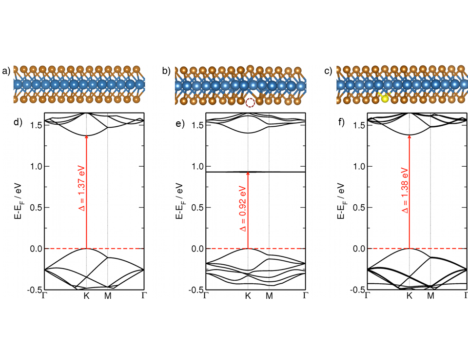 Figure 1
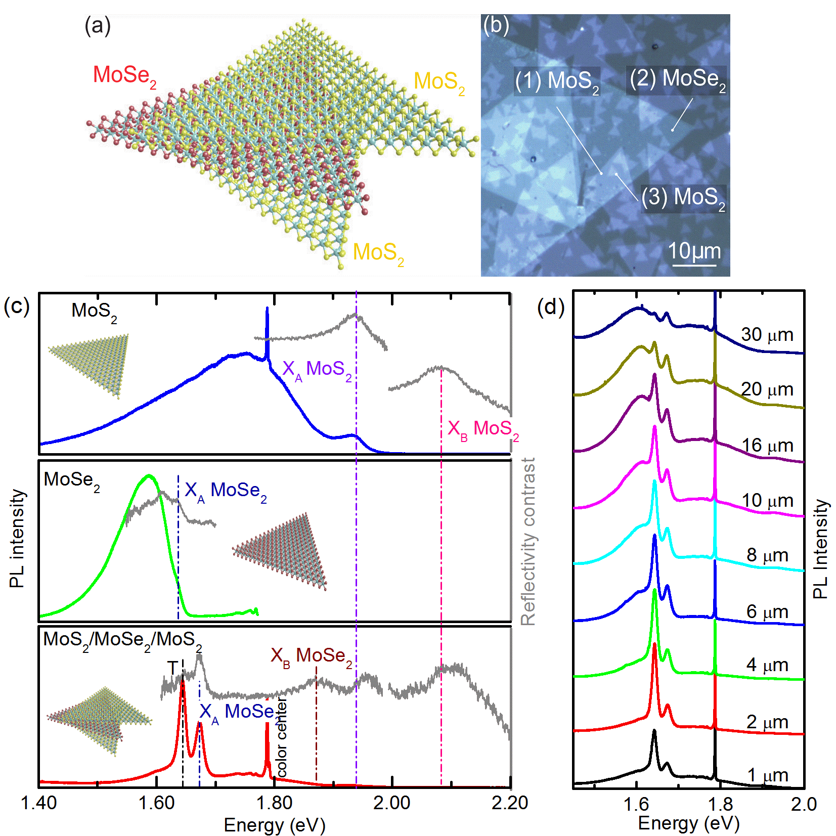 Figure 1
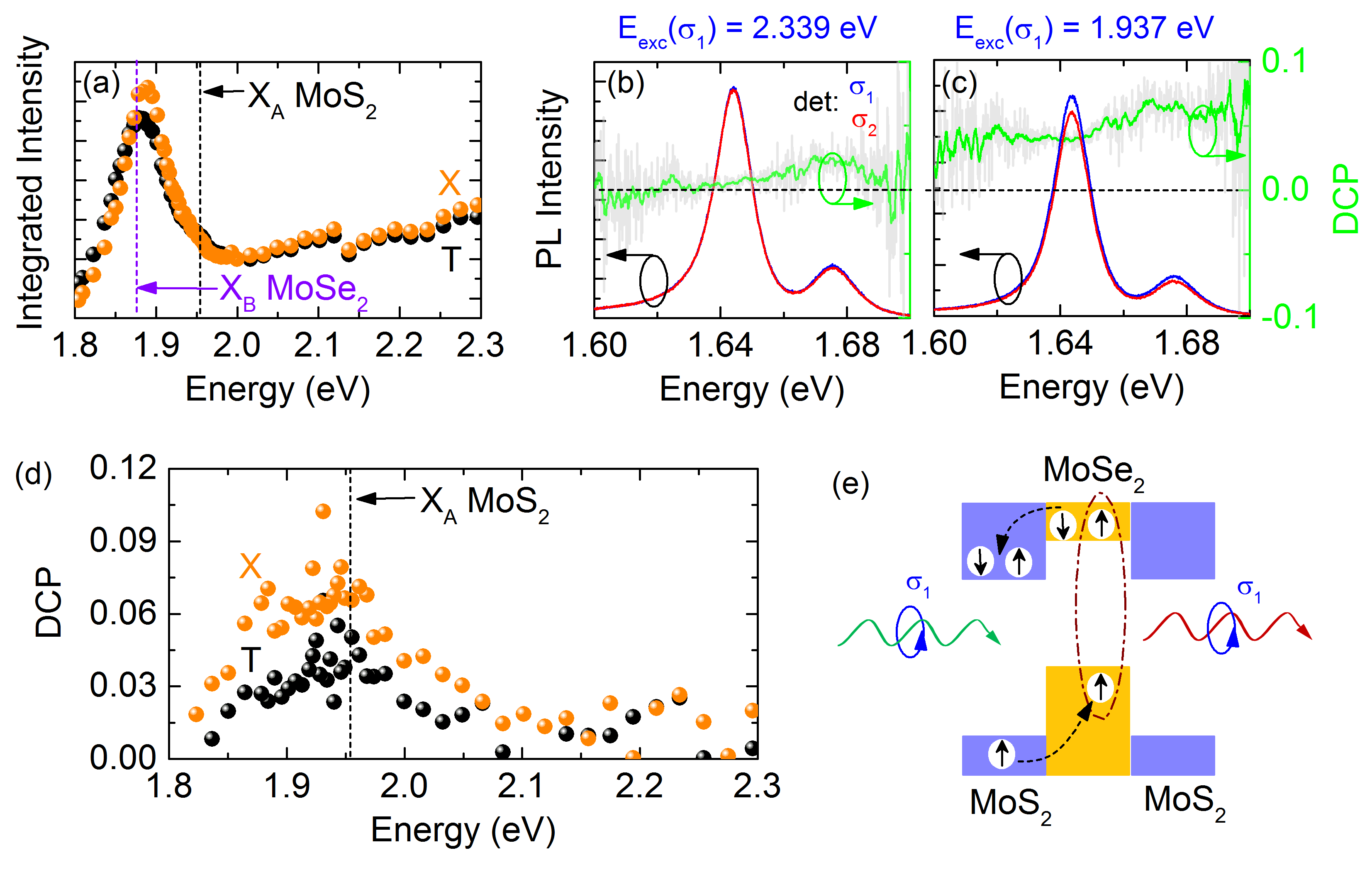 Figure 4
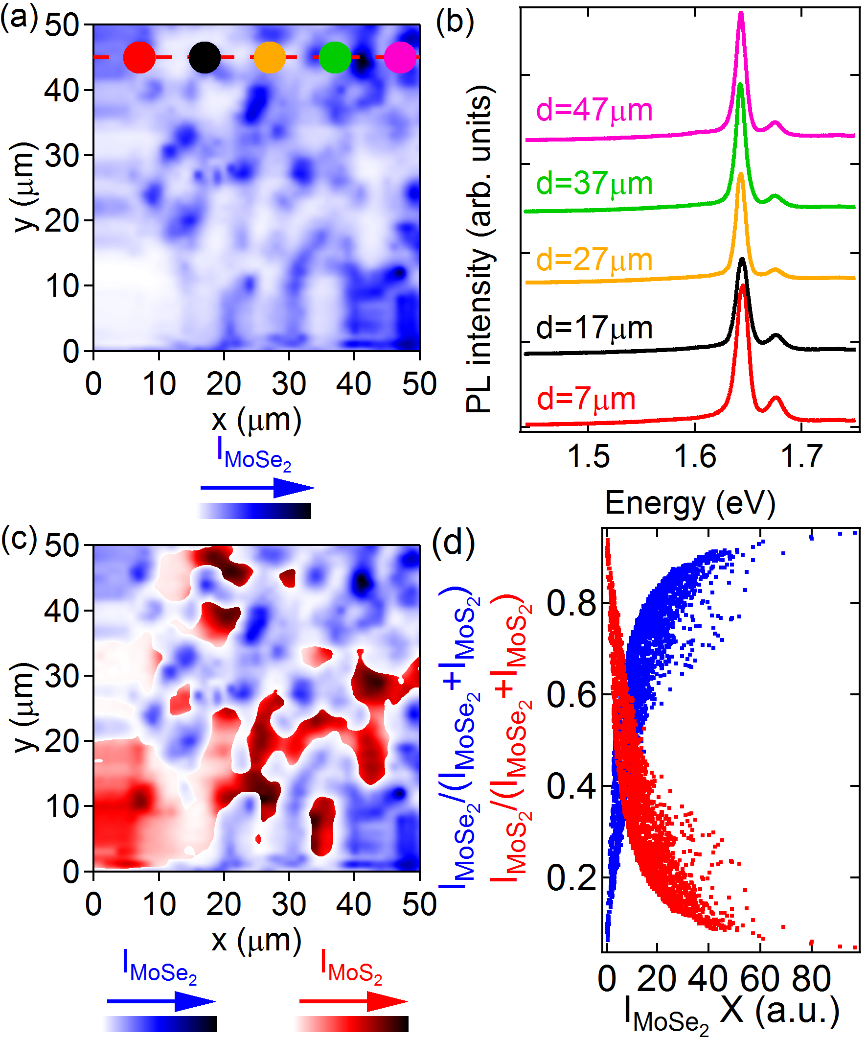 Figure 4
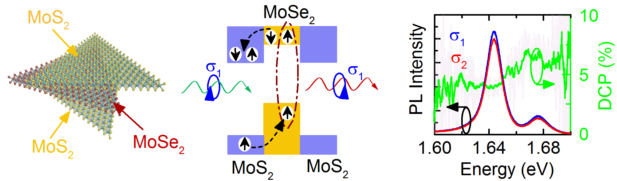 Figure 5
| System | () | () |
|---|---|---|
| MoS2 1L | 3.171 | - |
| MoSe2 1L | 3.251 | - |
| MoS2/MoSe2 | 3.214 | 6.21 |
| Model 1 | 3.206 | 6.30 |
| Model 2 | 3.203 | 6.26 |
Peer Reviews
No public reviews on file for this paper yet. If you reviewed it on a platform where reviews are public (OpenReview, ICLR, NeurIPS, ICML), you can paste yours below so the community can read it here.
Videos
No videos yet. Explain this paper in a talk, walkthrough, or lecture? Add one.
Defect healing and charge transfer mediated valley polarization in
MoS2/MoSe2/MoS2 trilayer van der Waals heterostructures
Alessandro Surrente
Laboratoire National des Champs Magnétiques Intenses, UPR 3228, CNRS-UGA-UPS-INSA, Grenoble and Toulouse, France
Dumitru Dumcenco
Electrical Engineering Institute and Institute of Materials Science and Engineering, École Polytechnique Fédérale de Lausanne, CH-1015 Lausanne, Switzerland
Zhuo Yang
Laboratoire National des Champs Magnétiques Intenses, UPR 3228, CNRS-UGA-UPS-INSA, Grenoble and Toulouse, France
Agnieszka Kuc
University of Leipzig, Wilhelm Ostwald Institute of Physical and Theoretical Chemistry Leipzig, Saxony, Germany
School of Engineering and Science, Jacobs University Bremen, Campus Ring 1, 28759 Bremen, Germany
Yu Jing
University of Leipzig, Wilhelm Ostwald Institute of Physical and Theoretical Chemistry Leipzig, Saxony, Germany
School of Engineering and Science, Jacobs University Bremen, Campus Ring 1, 28759 Bremen, Germany
Thomas Heine
University of Leipzig, Wilhelm Ostwald Institute of Physical and Theoretical Chemistry Leipzig, Saxony, Germany
School of Engineering and Science, Jacobs University Bremen, Campus Ring 1, 28759 Bremen, Germany
Yen-Cheng Kung
Electrical Engineering Institute and Institute of Materials Science and Engineering, École Polytechnique Fédérale de Lausanne, CH-1015 Lausanne, Switzerland
Duncan K. Maude
Laboratoire National des Champs Magnétiques Intenses, UPR 3228, CNRS-UGA-UPS-INSA, Grenoble and Toulouse, France
Andras Kis
Electrical Engineering Institute and Institute of Materials Science and Engineering, École Polytechnique Fédérale de Lausanne, CH-1015 Lausanne, Switzerland
Paulina Plochocka
Laboratoire National des Champs Magnétiques Intenses, UPR 3228, CNRS-UGA-UPS-INSA, Grenoble and Toulouse, France
Abstract
Monolayer transition metal dichalcogenides (TMDC) grown by chemical vapor deposition (CVD) are plagued by a significantly lower optical quality compared to exfoliated TMDC. In this work we show that the optical quality of CVD-grown MoSe2 is completely recovered if the material is sandwiched in MoS2/MoSe2/MoS2 trilayer van der Waals heterostructures. We show by means of density-functional theory that this remarkable and unexpected result is due to defect healing: S atoms of the more reactive MoS2 layers are donated to heal Se vacancy defects in the middle MoSe2 layer. In addition, the trilayer structure exhibits a considerable charge-transfer mediated valley polarization of MoSe2 without the need for resonant excitation. Our fabrication approach, relying solely on simple flake transfer technique, paves the way for the scalable production of large-area TMDC materials with excellent optical quality.
keywords:
Chemical Vapor Deposition, transition metal dichalcogenides, van der Waals heterostructures, defect healing, charge transfer mediated valley polarization
{tocentry}
Monolayer transition metal dichalcogenides (TMDC) have a direct bandgap situated in the visible range, which makes them ideal building blocks for novel electronic and optoelectronic devices 1, 2, 3, 4, 5, 6, 7, 8, 9, 10. The bandgap of monolayer TMDCs occurs at the inequivalent (but degenerate) K and K’ points of the hexagonal Brillouin zone. The broken inversion symmetry of a TMDC monolayer combined with the time reversal symmetry imposes opposite magnetic moments at the K and K’ valleys. This in turn determines the characteristic circular dichroism exhibited by these materials, wherein each valley can be addressed separately with circularly polarized light of a given helicity 11, 12, 13. Additionally, optical spectra are influenced by the strong spin-orbit coupling, which lifts the degeneracy of band states at the valence band edges, resulting in well-resolved A and B resonances, as observed in reflectivity or absorption spectra 2, 14, 15, 16. The interplay of spin-orbit coupling with broken inversion symmetry and time reversal symmetry locks the valley and spin degrees of freedom, making TMDC attractive candidates for valleytronics 17. The spin-valley index locking along with the large distance in the momentum space between K and K’ valleys preserves the valley polarization observed in the degree of circular polarization (DCP) in helicity resolved photoluminescence emission18, 19, 20, 21, 22.
Applications require a scalable fabrication platform providing high-quality large-area monolayer TMDC. Unfortunately, the most promising approach today, namely chemical vapor deposition (CVD) growth23, 24, 25, 26, 27 struggles to compete with exfoliated TMDC in terms of sample quality. Low temperature PL spectroscopy of CVD-grown MoS2 and MoSe2 reveals broad emission from defect bound excitons, which is significantly more intense than the free exciton peak 28, 29, 30 and is related to chalcogen vacancies induced during the CVD growth 29, 30.
Here, we demonstrate a novel approach to neutralize the intrinsic defects of CVD-grown TMDCs, using flake transfer tools routinely employed in the fabrication of van der Waals heterostructures 31, 32, 33. We investigate the optical properties of trilayer stacks composed of external CVD-grown MoS2 flakes 24 as capping layers and an internal CVD-grown MoSe2 flake which has a smaller bandgap 34, 35. Remarkably, this fabrication approach strongly suppresses the localized exciton emission in MoSe2, yielding a low temperature PL comparable to that observed in mechanically exfoliated samples. This striking result can be understood from density functional theory (DFT), which suggests that the more reactive MoS2 donates chalcogen atoms to heal vacancy defects in MoSe2. Incorporating MoS2 into the trilayer heterostructure furthermore allows us to demonstrate a new way to introduce valley polarization in MoSe2. Due to the type II band alignment in TMDC heterojunctions 35, a significant charge transfer is observed in these systems 36, 37, 32. Our results show that spin of the hole is conserved upon charge transfer from MoS2 to MoSe2 after excitation in resonance with MoS2 A exciton. This leads to non-zero steady state valley polarization in MoSe2, which has never been observed before under non-resonant excitation 38, 39, 40.
1 Defect healing
The sample with MoS2/MoSe2/MoS2 trilayer stacks and micrograph of a representative transfer area are schematically shown in Fig. 1(a) and (b). Low temperature microPL (PL) spectroscopy has been used to characterize as-grown CVD samples on the sapphire substrate (prior to any transfer process) and the trilayer MoS2/MoSe2/MoS2 stack. All spectra shown in Fig. 1(c) and (d) were measured under nominally identical conditions with an excitation power of (see Fig. S1 in Supporting Information (SI) for power dependent PL spectra). The as-grown MoS2 and MoSe2 monolayers both show a broad PL feature (full width at half maximum, FWHM, of and , respectively) related to emission from excitons bound to defect or charge impurity states 28, 41, 29, 30. A-exciton emission (labeled X in Fig. 1(c)) is seen only as a weak peak or shoulder at higher energies. These assignments are confirmed by reflectivity contrast measured on the same spot. Reflectivity contrast is defined as , where is the reflectivity spectrum measured on the sample and denotes the reflectivity spectrum measured on the substrate. In the case of transparent substrates such as sapphire, reflectivity contrast is proportional to the absorption of the sample 42. The reflectivity contrast spectrum of as-grown MoS2 (see upper panel of Fig. 1(c)) consists of a main peak at and a higher energy, weaker feature at , related to the spin-orbit split B exciton. The energy difference of corresponds very well to theoretically predicted spin-orbit splitting of the valence band 43 and is very similar to the splitting determined with transmission measurements on similar samples 34. The reflectivity contrast spectrum of as grown MoSe2, shown in the central panel of Fig. 1(c) has a peak at , which corresponds well to the high energy shoulder of the PL spectrum and hence is assigned to A exciton. As in our previous study 34, we are unable to resolve the B exciton in reflectivity contrast measurements on as grown MoSe2.
The optical properties of the trilayer stack are dramatically improved (bottommost panel in Fig. 1(c)). The most striking difference is the nearly total suppression of (i) emission from defect bound excitons, and (ii) significant quenching of both MoS2 PL, barely seen as a weak peak at , and of MoSe2 PL (overall integrated intensity decrease by two and one orders of magnitude, respectively, see Fig. S2 in SI). The measured PL spectrum is dominated by narrow free neutral (X) and charged exciton (T) emission in MoSe2 (low power FWHM of and , respectively, see Fig. S1 in SI), approaching the quality of exfoliated WSe2 embedded in boron nitride (FWHM 10\text{,}\mathrm{meV}$$) 44. The free exciton emission overlaps with a weak broad background emission from the sapphire substrate (the narrow peak just below corresponds to the emission from a color center in sapphire). The highest energy peak in the reflectivity contrast spectrum of the trilayer (see Fig. 1(c), bottom panel), blue shifted with respect to the A exciton peak of MoS2 by is attributed to the B exciton of MoS2. The peak related to MoS2 A exciton in the reflectivity contrast spectrum is blue shifted by with respect to the corresponding PL peak. This Stokes shift has been attributed to the presence of a high doping level in MoS2 16, also present in our layers 45. On the low energy side of the PL spectrum, the two distinct peaks at and are assigned to the A exciton and to the trion of MoSe2, respectively. The trion binding energy of is very similar to that reported in other studies on MoSe2 29, 46.
The high optical quality of the MoSe2 embedded in the heterostructure enabled us to resolve an additional peak at in the reflectivity contrast spectrum, assigned to the B exciton of MoSe2 43, 47. The vastly improved optical properties suggest a defect healing process, in which the contact with MoS2 is enough to drastically reduce the number of defects in MoSe2. The quenching of the intralayer emission 32, 37 in the trilayer is manifestation of a fast charge transfer mechanism 36, 48 related to the type II band alignment in MoS2/MoSe2 heterostructures 35. The weak luminescence of MoS2 is consistent with a background n doping 45 of the as grown layers and with an additional charge transfer after the formation of the heterostructure. We assign the brighter emission from MoSe2 (in the trilayer) to the hole transfer to an intrinsically n doped material and to the defect healing effect, combined with luminescence resulting from higher energy states, similar to hot luminescence of direct exciton in multilayer MoSe2 49, 50. The long range optical uniformity of the trilayer stacks has been monitored by acquiring PL with a gradually defocused excitation beam. The acquired PL spectra are displayed in Fig. 1(d). For an excitation spot size of , the defect emission remains strongly suppressed. For larger spot sizes, a broad low-energy peak starts to emerge, probably due to defect related emission in MoSe2 in areas which are not fully capped. These measurements are a proof of concept, demonstrating that this approach, when optimized, should enable the fabrication of large area CVD-grown heterostructures with excellent optical quality.
Previous attempts at improving the optical properties of CVD-grown MoSe2 using HBr treatment 29 or the isoelectronic impurity substitution 30 have met with only partial success: Impurity-bound excitons still remained the most prominent component of the emission spectrum. Low temperature PL spectra consisted in broad features, wherein free exciton emission could be identified only after fitting. The optical properties of exfoliated MoS2 have been improved by superacid treatment 51. In our case, the simple act of bringing MoSe2 in intimate physical contact with MoS2, a procedure that can be performed after growth and does not require any chemical functionalisation, results in a virtually complete suppression of emission from the impurity-bound states and a spectrum in which the trion and exciton resonances can be clearly resolved.
Our defect healing hypothesis is further supported by the results obtained from DFT simulations. We have calculated the gain of energy in a heterobilayer MoSe2/MoS2 using two models: A single Se vacancy in the MoSe2 layer (Model 1) and a single S vacancy in the MoS2 layer together with a single S substitution in the MoSe2 layer (Model 2). This corresponds to the transfer energy of a S atom from pristine MoS2 to heal a defect in MoSe2. We observe a significant energy gain of 18 kJ mol*-1* (180 meV) per S transfer from MoS2 to the MoSe2 defect, which shows that defect healing in MoSe2 by MoS2 is thermodynamically favored. The formation energy of a S vacancy in a MoS2 monolayer has been theoretically estimated in the – range 52, 53. We consider these as upper bounds for the energy barrier of the transfer of a S atom to fill a Se vacancy in MoSe2, because this is not a static process but a transfer between two neighbouring layers.
We have also calculated the band structures of a perfect MoSe2 monolayer, MoSe2 monolayer with one Se vacancy, and MoSe2 monolayer with one SeS substitution. We observe that Se vacancies introduce strongly localized states in the bandgap of MoSe2, 0.92 eV above the top of the valence band (see Fig. 2). These are dispersionless and act as trap centers. Healing the Se vacancy with S substitution restores the band structure of a nearly perfect MoSe2 monolayer. In the studied supercell model (2 SeS substitutions), the bandgap increases by only 1 meV.
2 Charge transfer mediated valley polarization
First signatures of charge transfer between the layers are seen in the comparison between PL intensities of as grown layers and trilayers, shown in Fig. S2 of SI. Additional insights is provided by the spatial correlation of the PL intensity of the MoS2 and MoSe2. The integrated spatial map of the MoSe2 A exciton is shown in Fig. 3(a). The signal is particularly intense at positions where the overlap between the three layers is good and the material does not have a large number of defects. This implies that the bright spots do not necessarily have a triangular shape. This map provides an additional opportunity to demonstrate the high degree of uniformity of the emission of MoSe2 incorporated in a heterostructure, by extract PL spectra. We show in Fig. 3(b) five PL spectra measured at distance from one another. The spectra have been normalized by the integration time. We note that emission from defect states is consistently absent in the five spectra and the similar line shape points to a good uniformity of the emission over the full mapped area. In Fig. 3(c), we overlay the intensity map of MoS2 with that of MoSe2, forcing the areas having the lowest signal from the latter to be transparent. These areas correspond to zones where the signal from MoS2 is highest. We quantify the observed intensity (anti)correlation by plotting in Fig. 3(d) the ratio between the intensity of A exciton in one material normalized by the total emission of both materials [), where = S or Se]. It can be noted that when the emission of MoSe2 becomes more pronounced, the emission of MoS2 decreases correspondingly. This is fully consistent with charge transfer. In positions where the three layers overlap efficiently, charge transfer induces a quenching of the MoS2 PL. At the same time, the PL from MoSe2 is particularly intense at these positions owing to efficient defect healing, but still weaker than in as grown MoSe2 samples (see Fig. S2 in SI).
Photoluminescence excitation (PLE) spectroscopy is a useful tool to investigate more thoroughly the charge transfer processes. We focus our measurements on MoSe2 incorporated in a trilayer stack. In Fig. 4(a), we show the PLE measured without making use of polarization optics. Both PLEs of the A exciton and trion have been normalized by the weakest intensity measured at an excitation energy of 1.999 eV in order to be able to compare the enhancement effects for the exciton and trion. The integrated intensities of both peaks show a pronounced maximum when the excitation energy is close to the resonance with the B exciton of MoSe2 54. The integrated intensity is consistently lower than this maximum at other excitation energies, including those corresponding to resonances in MoS2 (see for example the weak peak corresponding to MoS2 X, appearing as a shoulder of the main PLE peak in Fig. 4(a)). This is the exact opposite of what is observed in a heterostructure system where energy transfer has been demonstrated. In such system, the emission intensity of one material is significantly enhanced when the excitation energy is resonant with excitonic transitions of the other material 55. This consideration allows us to safely rule out energy transfer between the different layers.
To investigate whether the trilayer stack shows charge transfer, we initially consider the normalized intensity of exciton and trion when the excitation energy is resonant with excitonic transitions of MoS2. For resonances with both A and B exciton of MoS2, the emission intensity is enhanced more for MoSe2 A exciton than for the trion. This is consistent with the presence of a large n-type background doping (free electrons) in CVD-grown MoSe2, which gives rise to strong charged exciton emission even in the absence of gating (see Fig. 1(a)). For a MoS2/MoSe2 heterojunction, the band alignment promotes the transfer of holes from MoS2 to MoSe2 35. When we optically excite the trilayer stack, we induce a net transfer of holes from MoS2 to MoSe2, resulting in a relatively stronger emission of the neutral exciton as compared to the trion 55.
We also performed circular polarization resolved PLE focusing on MoSe2 incorporated in a trilayer stack. When the excitation energy is far from resonance (A or B excitons of both materials), MoSe2 shows an extremely small valley polarization. This is illustrated by the polarization-resolved PL spectra of Fig. 4(b), where a negligibly small DCP, defined as , is observed across the entire energy range of interest 38. When the excitation energy of the laser was tuned to the proximity of the resonance with the A exciton of MoS2, a significant valley polarization accumulates. An example of polarization resolved spectra at an excitation energy resonant with A exciton of MoS2 is shown in Fig. 4(c). The valley polarization is quantified by a slightly positive DCP at energies around A exciton and trion of MoSe2 (see Fig. 4(c)). In Fig. 4(d) we illustrate the excitation energy dependence of the integrated DCP (estimated by extracting the relevant integrated intensity of exciton and trion with Gaussian fits). We notice a significant increase of the integrated DCP at energies corresponding to the A exciton resonance of MoS2 (see dashed line in Fig. 4(d)), with a low energy shoulder possibly related to an enhanced DCP at excitation energies corresponding to MoSe2 B exciton 38. Polarization resolved electroluminescence of single and multilayer MoSe2 56 as well as polarization resolved PL of indirect excitons emitted by a WSe2/MoSe2 heterostructure 57 have demonstrated higher degree of circular polarization. However, the mechanisms leading to polarized emission in these systems are fundamentally different from those yielding polarized PL of MoSe2 56, which is virtually impossible to achieve unless the PL is excited using quasi-resonant excitation in X of MoSe2 38, 39, 40.
We ascribe the observed MoSe2 valley polarization to the hole transfer from MoS2, with a mechanism schematically illustrated in Fig. 4(e). We excite the trilayer stack with circularly polarized light with a given helicity and in resonance with the A exciton of MoS2. The valley polarization directly created in MoSe2 is quickly lost, which results in a negligible DCP, similarly to non-resonant excitation (see Fig. 4(d)). Resonant excitation in MoS2 creates valley polarization for a duration estimated in the hundreds of femtoseconds range 58. Charge transfer in van der Waals heterostructures is an ultra fast process, with upper bounds in the tens of femtoseconds range (hole transfer from MoS2 has been reported to be faster than 36). During this very rapid transfer, we assume that the hole spin (and thus valley due to the large spin orbit splitting in the valence band) is conserved, and, owing to the excess electron population in the MoSe2 layer, the injected hole forms an exciton populating the valley corresponding to the helicity of the incoming light. These excitons have presumably a low kinetic energy (no excess energy of the photocreated hole), which slows down significantly the inter-valley scattering rate due to electron-hole exchange interaction 59. As a result, this hole transfer is responsible for the observed valley polarization.
3 Conclusions
A detailed investigation of the optical properties of MoS2/MoSe2/MoS2 trilayers reveals that stacking dramatically improves the optical quality of CVD-grown MoSe2, essentially eliminating all defect bound exciton and MoS2-related emission. These results open the way to using CVD-grown TMDCs for applications and studies that require materials with excellent optical quality. Photoluminescence spectra from MoSe2 in a trilayer stack are dominated by narrow neutral and charged A exciton emission, resembling the spectrum of a high quality mechanically exfoliated flake. Density functional calculations confirm a defect healing scenario in which S atoms replace Se vacancies. Circular polarization resolved PL measurements demonstrate that MoSe2 exhibits a significant valley polarization even when the excitation energy is far from the A exciton resonance. This behavior is the signature of an efficient spin-conserving hole transfer from MoS2 to MoSe2. Our approach provides a robust and straightforward method of healing defects in CVD-grown samples, which might also be beneficial for the transport properties of these materials.
4 Acknowledgments
This work was partially supported by ANR JCJC project milliPICS, the Région Midi-Pyrénées under contract MESR 13053031, BLAPHENE project under IDEX program Emergence, “Programme des Investissements d’Avenir” under the program ANR-11-IDEX-0002-02, reference ANR-10-LABX-0037-NEXT, Swiss SNF Sinergia Grant no. 147607, the European Commission (ITN MoWSeS, GA 317451), and Deutsche Forschungsgemeinschaft (HE 3543/27-1 and GRK 2247/1 (QM3)). Y.J., A.K. and T.H. thank ZIH Dresden for supercomputer time. This project has received funding from the European Union’s Horizon 2020 research and innovation programme under grant agreement No. 696656 (Graphene Flagship).
{suppinfo}
Supporting information: Low temperature PL spectra, comparison of PL spectra of as-grown versus trilayer samples, temperature dependent PL spectra and time-resolved PL.
5 Methods
5.1 Sample preparation
The sample with MoS2/MoSe2/MoS2 trilayer stacks, schematically shown in Fig. 1(a), was obtained by two separate transfer steps using a wet transfer KOH method 32. First of all, the upper-MoS2 was transferred onto the as-grown MoSe2 monlayer on sapphire 24, 34. Subsequently, the MoS2/MoSe2 stack was transferred onto an as-grown bottom MoS2 monolayer on sapphire. For both transfers, sapphire chips with material (upper-MoS2 or MoS2/MoSe2 stack) were first spin coated with PMMA 950 at 1500 rpm for and baked at for 5 minutes. The films were detached in KOH (30%) at moderate temperatures (), washed 3 times in deionized water, transferred onto sapphire with the stacking layer (MoSe2 or bottom-MoS2) and dried at for 30 minutes. The PMMA was removed by dipping the sample in acetone for 12 hours, followed by rinsing with isopropanol and drying in a N2 flow. Such method provides a polymer clean interface of stacks and minimal damage of material caused by the transfer process. Using this method, a large area film with monolayer (MoS2), bilayer (MoSe2/MoS2, MoS2/MoS2 and MoS2/MoSe2 stacks) and trilayer (MoS2/MoSe2/MoS2 stack) was obtained. A micrograph of a representative transfer area is shown in Fig. 1(b). To determine the position of areas with different number of stacked layers, Ni markers were deposited.
5.2 Optical measurements
For the optical characterization, the sapphire substrate was mounted on the cold finger of a He-flow croystat. The excitation was provided either by a CW frequency doubled solid state laser emitting at or by the frequency doubled output of an optical parametric oscillator (OPO), synchronously pumped by a mode-locked Ti:sapphire laser. The typical temporal pulse width was , with a repetition rate of . The excitation beam was focused on the sample by a microscope objective, giving a spot size of approximately and having a numerical aperture of 0.55. The emitted PL was collected through the same objective and redirected to a spectrometer equipped with a liquid nitrogen cooled CCD camera or (for time-resolved measurements) to an imagining spectrometer and detected using a synchroscan streak camera with the temporal resolution set to . All the spectra have been measured at , unless otherwise specified.
For spatial mapping the emission has been monitored while the optical cryostat was displaced with respect to the microscope objective using high precision motorized translation stages ( step). The integrated intensity of given features (e.g. A exciton emission) has been obtained by performing Gaussian fitting of the measured PL spectra.
5.3 Density functional theory of band structure in MoSe2/MoS2 heterobilayers
We have calculated heterobilayers made of MoSe2 and MoS2 monolayers, using DFT as implemented in the Crystal09 software60. We employed all-electron Gaussian-type bases of triple-quality61, 62, while Mo atoms were treated with the HAYWSC-311(d31)G basis with effective core potential set63, together with the PBE gradient corrected density functional64. London-dispersion interactions were accounted for using the approach proposed by Grimme (DFT-D3)65. Full optimization of atomic positions and lattice vectors was performed on both models: Model 1 with perfect MoS2 monolayer and one Se vacancy in the MoSe2 monolayer, and Model 2 with one S vacancy in the MoS2 monolayer and one S substitution in the MoSe2 monolayer. The models are built of supercells (see Fig. 2).
Geometry optimization only slightly alters the lattice geometry (see Table 1).
For the large supercells, which still overestimate the defect density in experiment, the defects studied here do not introduce any drastic changes into the structural properties of the systems. However, we note that we are constrained with the commensurate models of a heterobilayer, in which the corresponding monolayers are slightly distorted compared with the relaxed monolayers and for MoSe2 and MoS2, respectively. For a perfect heterobilayer (), this gives compression of MoSe2 and elongation of MoS2.
The reference list from the paper itself. Each links out to its DOI / PubMed record.
- 1Splendiani et al. 2010 Splendiani, A.; Sun, L.; Zhang, Y.; Li, T.; Kim, J.; Chim, C.-Y.; Galli, G.; Wang, F. Nano Letters 2010 , 10 , 1271–1275
- 2Mak et al. 2010 Mak, K. F.; Lee, C.; Hone, J.; Shan, J.; Heinz, T. F. Physical Review Letters 2010 , 105 , 136805
- 3Radisavljevic et al. 2011 Radisavljevic, B.; Radenovic, A.; Brivio, J.; Giacometti, V.; Kis, A. Nature Nanotechnology 2011 , 6 , 147–150
- 4Kuc et al. 2011 Kuc, A.; Zibouche, N.; Heine, T. Physical Review B 2011 , 83 , 245213
- 5Lopez-Sanchez et al. 2013 Lopez-Sanchez, O.; Lembke, D.; Kayci, M.; Radenovic, A.; Kis, A. Nature Nanotechnology 2013 , 8 , 497–501
- 6Baugher et al. 2014 Baugher, B. W.; Churchill, H. O.; Yang, Y.; Jarillo-Herrero, P. Nature Nanotechnology 2014 , 9 , 262–267
- 7Ross et al. 2014 Ross, J. S.; Klement, P.; Jones, A. M.; Ghimire, N. J.; Yan, J.; Mandrus D., G.; Taniguchi, T.; Watanabe, K.; Kitamura, K.; Yao, W.; Cobden, D. H.; Xu, X. Nature Nanotechnology 2014 , 9 , 268–272
- 8Pospischil et al. 2014 Pospischil, A.; Furchi, M. M.; Mueller, T. Nature Nanotechnology 2014 , 9 , 257–261