Neutral Helium Atom Diffraction from a Micron Scale Periodic Structure: Photonic Crystal Membrane Characterization
Torstein Nesse, Sabrina D. Eder, Thomas Kaltenbacher, Jon Olav, Grepstad, Ingve Simonsen, Bodil Holst

TL;DR
This paper demonstrates helium atom diffraction as a technique to characterize photonic crystal membranes with micron-scale periodic structures, extending the measurable period range beyond previous limits.
Contribution
The study presents the first helium diffraction measurements of a photonic crystal membrane with a 490nm period, significantly larger than prior diffraction limits, and introduces a model to interpret the data.
Findings
Largest period measured with helium diffraction to date (490nm)
Successful extraction of structural parameters from diffraction data
Validated model linking helium beam characteristics to diffraction patterns
Abstract
Surface scattering of neutral helium beams created by supersonic expansion is an established technique for measuring structural and dynamical properties of surfaces on the atomic scale. Helium beams have also been used in Fraunhofer and Fresnel diffraction experiments. Due to the short wavelength of the atom beams of typically 0.1nm or less, Fraunhofer diffraction experiments in transmission have so far been limited to grating structures with a period (pitch) of up to 200nm. However, larger periods are of interest for several applications, for example for the characterization of photonic crystal membrane structures, where the period is typically in the micron/high sub-micron range. Here we present helium atom diffraction measurements of a photonic crystal membrane structure with a two dimensional square lattice of 100x100 circular holes. The nominal period and hole radius were 490nm and…
Click any figure to enlarge with its caption.
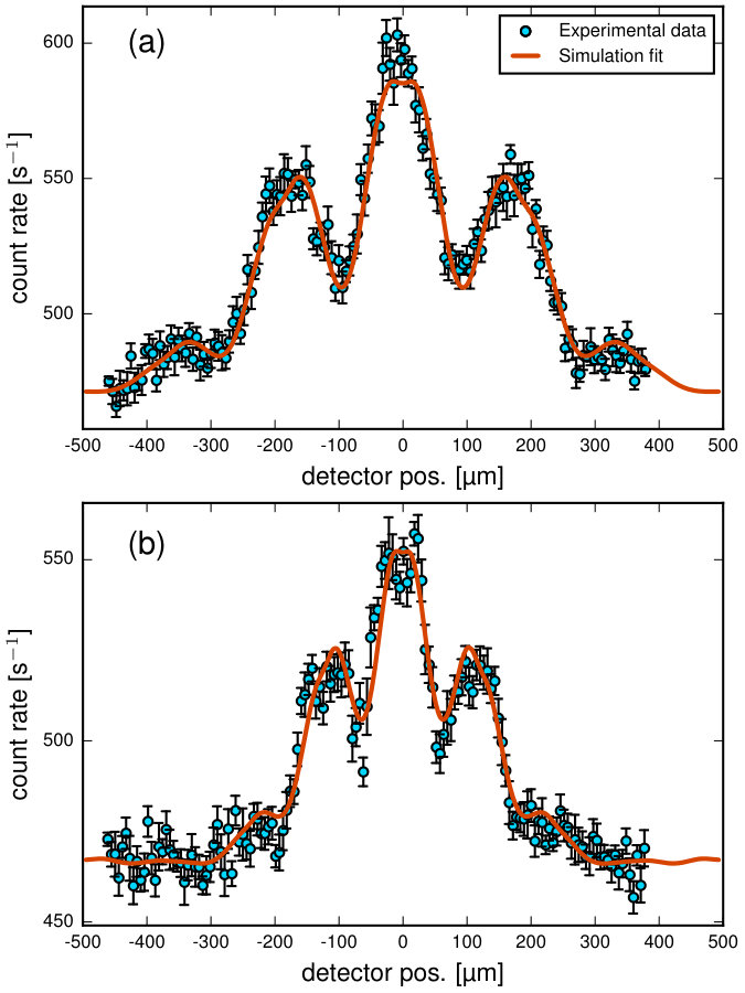 Figure 1
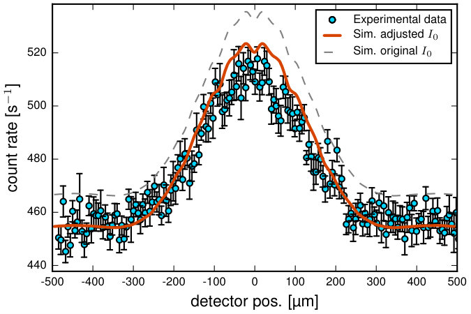 Figure 2
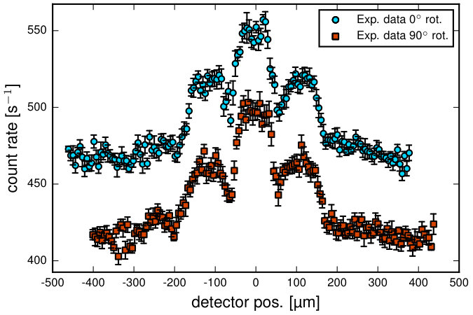 Figure 3
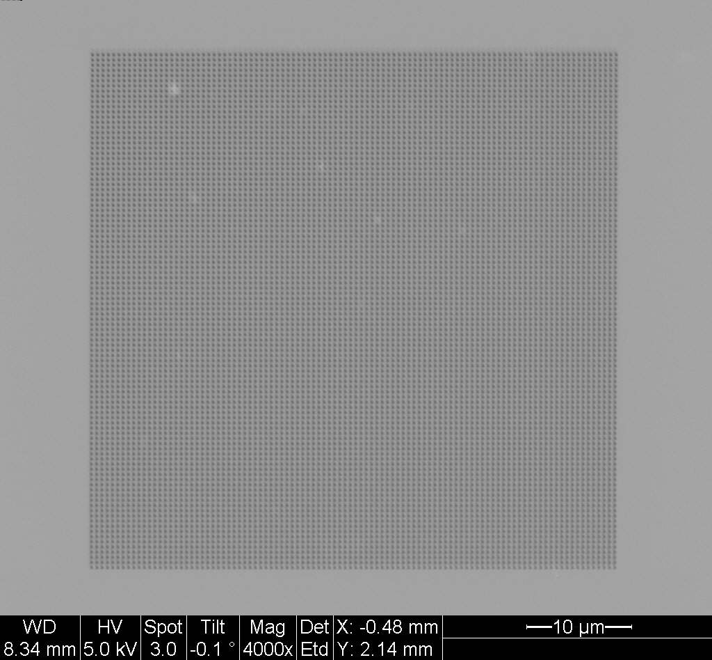 Figure 4
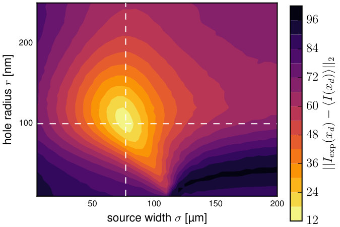 Figure 5
| Parameter | ||
|---|---|---|
| Wavlength [] | ||
| Source to sample distance [] | ||
| Skimmer radius [] | ||
| Hole radius [] | ||
| Hole periodicity [] | ||
| Sample to scan slit distance [] | ||
| Slit size | ||
Peer Reviews
No public reviews on file for this paper yet. If you reviewed it on a platform where reviews are public (OpenReview, ICLR, NeurIPS, ICML), you can paste yours below so the community can read it here.
Videos
No videos yet. Explain this paper in a talk, walkthrough, or lecture? Add one.
††thanks: T. Nesse and S. D. Eder contributed equally to this work††thanks: T. Nesse and S. D. Eder contributed equally to this work
Neutral Helium Atom Diffraction from a Micron Scale Periodic Structure: Photonic Crystal Membrane Characterization
Torstein Nesse
corresponding author [email protected]
Department of Physics, NTNU Norwegian University of Science and Technology, NO-7491 Trondheim, Norway
Sabrina D. Eder
corresponding author [email protected]
Department of Physics and Technology, University of Bergen, Allégaten 55, 5007 Bergen, Norway
Thomas Kaltenbacher
Department of Physics and Technology, University of Bergen, Allégaten 55, 5007 Bergen, Norway
Jon Olav Grepstad
Tunable InfraRed Technologies AS, Gaustadalleen 21, 0349 Oslo, Norway
Ingve Simonsen
Department of Physics, NTNU Norwegian University of Science and Technology, NO-7491 Trondheim, Norway
Surface du Verre et Interfaces, UMR 125 CNRS/Saint-Gobain, F-93303 Aubervilliers, France
Bodil Holst
Department of Physics and Technology, University of Bergen, Allégaten 55, 5007 Bergen, Norway
Abstract
Surface scattering of neutral helium beams created by supersonic expansion is an established technique for measuring structural and dynamical properties of surfaces on the atomic scale. Helium beams have also been used in Fraunhofer and Fresnel diffraction experiments. Due to the short wavelength of the atom beams of typically or less, Fraunhofer diffraction experiments in transmission have so far been limited to grating structures with a period (pitch) of up to . However, larger periods are of interest for several applications, for example for the characterization of photonic crystal membrane structures, where the period is typically in the micron/high sub-micron range. Here we present helium atom diffraction measurements of a photonic crystal membrane structure with a two dimensional square lattice of circular holes. The nominal period and hole radius were and respectively. To our knowledge this is the largest period that has ever been measured with helium diffraction. The helium diffraction measurements are interpreted using a model based on the helium beam characteristics. It is demonstrated how to successfully extract values from the experimental data for the average period of the grating, the hole diameter and the width of the virtual source used to model the helium beam.
pacs:
37.20.+j, 42.25.Fx
I Introduction
Helium atom scattering is a well-established technique in surface science. Elastic helium scattering is used to measure the structural properties of surfaces through diffraction and step height interference measurements. Inelastic helium scattering is used to measure surface dynamics properties such as diffusion and vibrations. The advantage of helium scattering lies in the very low energy of the beam (typically less than ) and the fact that the beam is neutral, which means that it is possible to investigate insulating and/or fragile surfaces and adsorbates. The small wavelength of the helium beam (less than ) means that it is very well suited for investigating structures on the atomic scale. Larger scale structures put severe demands on the beam collimation and angular resolution of the diffraction system. The largest period of a surface periodic structure that has been resolved using helium scattering is, to our knowledge, a surface reconstruction of -quartz (0001) with a period of Eder. et al. (2015). For reviews of the use of helium atom surface scattering in surface science see Refs. Farias and Rieder (1998); Holst. and Bracco (2013).
Transmission helium atom diffraction has so far been used only in a limited number of experiments. This is mainly due to the fact that the low energy of the helium atoms means that they do not penetrate any solid materials and hence transmission experiments can only be performed on porous structures. Experiments have been carried out on grating structures with a period of up to Schöllkopf and Toennies (1994); Grisenti et al. (1999), and various Fresnel diffraction and focusing experiments have been done using zone plates and a Poisson spot aperture Doak et al. (1999); Koch et al. (2008); Reisinger et al. (2009); Eder et al. (2015). In this paper we present the first experiment carried out on a two-dimensional lattice structure: A photonic crystal membrane structure with a nominal period of and a hole radius of .
Photonic crystals have a number of potential applications Joannopoulos et al. (1997). They have been demonstrated as building blocks in integrated circuits Kuramochi et al. (2014), can be used as mirrors in applications requiring very high optical power or operating temperatures above a couple of hundred degrees Celsius Jeong et al. (2013), and are applied in the fabrication of quantum dots and quantum light sources applicable in quantum computing Lodahl et al. (2015). The commercial use of photonic crystals is currently limited to transducer elements in biosensors Cunningham et al. (2016) and to maximize the light extraction efficiency of light emitting diodes (LED) Matioli and Weisbuch (2010). The particular type of photonic crystal structure investigated in this paper was developed for the detection of single molecules Grepstad et al. (2012), and so it was particularly important to know if it was really transparent to atoms. This can be difficult to determine from a scanning electron microscope image, since the electrons may still penetrate nanometer thick residue layers making the sample appear transparent in a region where it in reality is not.
II Experimental setup
The photonic crystal membrane sample characterized in these experiments was composed of an array of through holes in a free-standing membrane, suspended in a silicon frame. The thickness of the membrane was and made of silicon nitride and silicon oxide thin films ( Si3N4 - SiO2 - Si3N4). The holes were made using electron beam lithography combined with reactive ion etching. The pattern consisted of a square array of circular holes. Each hole had a radius of and the grid had a period of , giving a patterned area containing a total of holes. A SEM image of the crystal is presented in Fig. 1. For a detailed description of the preparation see Ref. Grepstad et al. (2012).
The diffraction measurements were carried out using the molecular beam apparatus MAGIE Apfolter (2005). A diagram of the experimental setup is presented in Fig. 2. The helium beam was created by supersonic expansion through a diameter nozzle and collimated with a wide circular skimmer. Measurements were carried out using both a room temperature and a cooled beam, both with a stagnation pressure of . The former had a beam temperature of , corresponding to a wavelength of with a spread of . The cooled beam had a beam temperature of , corresponding to a wavelength of with a spread of . The photonic crystal sample was placed in the beamline a distance z_{ss}=$$1528\pm 5\text{\,}\mathrm{mm} after the skimmer. A wide vertical slit was placed a distance z=$$1044\pm 5\text{\,}\mathrm{mm} after the sample just in front of the detector. This slit was then moved horizontally in steps of approximately along the direction to scan the diffraction pattern.
Care was taken to align the sample so that it was perpendicular to the incident beam and to align one of the axes of the photonic crystal with the scan direction . We estimate that the alignment is precise to within . To test the overall configuration the sample was rotated and around its normal from the initial alignment and additional room temperature measurements were performed. To reduce background contributions to the measured signal, two collimating apertures were inserted before and after the sample at distances (AP1, diameter) and (AP2, diameter) from the sample. The second aperture AP2 was moved along with the slit in front of the detector when scanning. Even with these precautions the signal to background ratio was still not optimal. For the different measurements performed at , the maximum count rate was and the minimum count rate was , which corresponds to the strength of the fundamental peak and the background respectively. The final diffraction patterns presented here were made by averaging over a total of individual scans across the diffraction pattern.
III The diffraction model
III.1 Diffraction grating
Since the distances between the source and the sample, and between the sample and the detector are very large compared to the size of the grid and the wavelength of the beam, the Fraunhofer approximation is valid and we can model the propagation of the helium beam as a scalar wave. We look at the propagation of the scalar beam from a plane sample to a scanning plane parallel to the sample. In the Fraunhofer approximation, the diffracted field at position behind a single circular hole centered at position can be described by Goodman (2005)
[TABLE]
In this equation is the incident wavenumber, is the wavelength, is the radius of the hole, is the distance from the sample plane to the scanning plane, is the area of the hole and is the incident field at the sample. A position in-plane with a normal in the propagation direction is denoted . The incident field changes across the sample, but we assume that it is approximately constant across a single hole.
To model the result of the diffraction grating we take the superposition of the fields found using Eq. (1) for each hole in the two-dimensional grid of holes:
[TABLE]
where is the hole coordinate in the grid (), and is the hole position.
To relate the field to the measured quantity we glide a slit over the intensity in the scanning plane , and integrate over the intensity inside the slit at each position. This leads to a quantity similar to the one captured in the experiment
[TABLE]
where is the center position of the slit along the scanning direction , and and is the width and the height of the scanning slit respectively.
III.2 Source description
The supersonic source gives rise to an incoherent beam of helium atoms with a narrow speed distribution. In principle, the speed distribution will cause the diffraction pattern to “smear out” due to the difference in wavelength; however, in the experimental results that we will present, the speed distribution is so narrow that this effect is not very prominent. A change in wavelength equal to the spread given in Sec. II shifts the position of the first order diffraction peaks by approximately . Hence, in the following, the beam will be assumed to be characterized by the wavelength that corresponds to its center energy (or speed).
To describe the Helium source used in the experiments we will adapt the virtual source model that was introduced by Beijerinck and Verster to describe supersonic expansions Beijerinck and Verster (1981). Here, the atoms initially collide until they eventually reach the molecular flow regime at a distance from the nozzle referred to as the quitting surface. When this happens, the individual trajectories can be traced back to a plane that is perpendicular to the mean direction of travel and where the width of the spatial distribution function of the trajectories is at a minimum — the virtual source. This spatial distribution can be fitted with one or two Gaussian functions Beijerinck and Verster (1981); DePonte et al. (2006).
Within the virtual source model, the incident beam is considered as an incoherent and weighted superposition of spherical waves (point sources) located approximately in the skimmer plane. Here, the weight (or amplitude) used in the superposition will be taken to be a Gaussian function whose width, called below, mimics the half width of the skimmer. Mathematically the incident field at position can therefore be written in the form
[TABLE]
where denotes a position in the skimmer plane and represents a random phase function associated with the spherical wave at . This function is assumed to be an uncorrelated stochastic variable that is uniformly distributed on the interval . The incident amplitude has been set to in Eq. (4).
To perform simulations using the incident field, the integral in Eq. (4) has to be evaluated numerically and the results that depend on it are averaged over an ensemble of realizations of the random phase function.
It will be seen in Sec. IV that the form of the incident field given by Eq. (4) is sufficient to explain the measured results.
III.3 Fit to experimental data
A rescaling is necessary to compare the results of the diffraction model described in Secs. III.1 and III.2 with the experimental data. The experimental data are captured as counts per second, which we must scale the simulation data to fit. The experimental data also contains a strong background signal. To take these effects into account we have fitted the results from the diffraction model to the experimental data using two variables; one for scaling the overall intensity to match the source intensity and one for shifting the results and taking the background into account ,
[TABLE]
Here is the mean over several realizations of the random phase function in Eq. (4). The best values for and were then found by a least squares fit of to the experimental data . The fit was performed using the error norm
[TABLE]
where is the standard error of the experimental measurements.
IV Results and Discussion
Helium diffraction intensity measurements in transmission were performed for beam temperatures and , and the results are presented as circles in Figs. 3(a) and 3(b), respectively. The presented measurements are the arithmetic mean of independent horizontal detector scans (-scans) for each beam temperature. The error bars reported for each experimental data point correspond to the standard deviation on the mean calculated for each point.
The measurements presented in Fig. 3 show pronounced diffraction patterns. The count rates for the zeroth and first order diffraction peaks are all more than higher than the background level. The observed diffraction patterns behave as expected: They are symmetric around the location of the fundamental order peak located at , and the positions and widths of the diffraction peaks vary with temperature. In particular, one observes that when the temperature of the incident beam is increased, the distance between the positions of the fundamental and the first diffractive orders and the widths of the peaks both become smaller. Since the wavelength associated with the beam of incidence is inversely proportional to the temperature of the beam (see Table 1), such behavior is expected from the grating equation from physical optics 111Under the assumption of normal incidence, the grating equation (in 1D for simplicity) reads where denotes the transmission angle of the diffraction order . Here and represent the wavelength of the incident beam and the lattice constant, respectively. For details the interested reader is referred to Ref. Goodman (2005).. We have checked that for the geometrical parameters used in the design of the experimental setup, the location of the first order diffraction peaks seen in Fig. 3 are observed at positions that are consistent with the predictions obtained from the grating equation for both beam temperatures.
We now turn to the modeling of the diffraction patterns that were obtained experimentally, which is performed on the basis of the virtual source diffraction model outlined in Sec. III; see Eqs. (3)–(6). The solid lines that appear in Fig. 3 represent the predictions of the diffraction model for the two beam temperatures considered. These results were obtained by averaging the results of realizations of the source. In order to produce these simulation results, the geometrical parameters characterizing the experimental setup, the sample, and the temperature (and wavelength) of the incident beam were assumed known. An overview of these parameters and their values is presented in Table 1.
It was found that the diffraction model produces diffraction patterns which forms are sensitive to the width of the virtual source , see Eq. (4). The widths of the diffraction peaks strongly depend on the shape of the incoming field. By changing the width in the source model, the width of the modeled diffraction peaks change. A wider Gaussian envelope used for the incident beam (a larger value for ) will broaden the diffraction peaks. In principle, the source width can be measured experimentally Reisinger et al. (2007); Eder et al. (2014). However, such measurements typically yield significant uncertainty on the source width. Therefore, we instead decided to determine this parameter by fitting the diffraction model to the experimental diffraction data based on Eq. (5) and the cost function Eq. (6). This means that the free parameters used in the diffraction model were the source width , the amplitude , and the background intensity , see Eq. (5). In this way the diffraction model was fitted to the measured data sets with respect to the parameter set . We discuss the roboustness of the fit at the end of this section.
From the results presented in Fig. 3 it is observed that the diffraction model from Sec. III is capable of representing the measured diffraction patterns well: both when it comes to the positions of the diffraction peaks, their widths, and the relative amplitudes of the peaks. The width of the virtual source was determined in the fitting procedure to be [Fig. 3(a)] and [Fig. 3(b)] for the beam temperatures and , respectively.
It is interesting to note that the values we obtained for when producing the numerical results (solid lines) shown in Fig. 3 do agree well with values reported previously in the literature for cooled and room temperature He beams Reisinger et al. (2007); Eder et al. (2014). The measurements reported in these references were conducted using a zone plate to image directly the virtual source. The beam temperatures used in these two studies were and , which is close to the temperatures used in our experiments to allow for a comparison. For the measurements done at room temperature, the size of the virtual source is usually described as the sum of two Gaussian functions with different widths. The size of the virtual source for a beam of temperature was reported in Ref. Reisinger et al. (2007). If the results from Ref. Reisinger et al. (2007) is fitted using a single Gaussian in order to more closely resemble the model used in this paper, one obtains 50\pm 10\text{,}\mathrm{\SIUnitSymbolMicro m}. This value should be compared to the result $\sigma=$52\text{\,}\mathrm{\SIUnitSymbolMicro m} that we report for the beam temperature obtained using the diffraction model Eqs. (3)–(5) and the experimental data reported in Fig. 3(b).
For a beam, the size of the virtual source is described with just one Gaussian. The lower level value reported in Ref. Eder et al. (2014) corresponds to \sigma=$$100\pm 10\text{\,}\mathrm{\SIUnitSymbolMicro m}. This is larger than the value \sigma=$$77\text{\,}\mathrm{\SIUnitSymbolMicro m} we obtained in the modeling for the beam temperature [Fig. 3(a)].
Since the grating in our sample is supposed to be square, a rotation of the sample around the -axis by an angle of [math] should, in principle, not alter the diffraction pattern that it produces. In Fig. 4 we present a comparison of two measured diffraction patterns for a beam temperature of (room temperature); the top data set corresponds to the original position of the sample (\phi=$$$) and the lower data set is collected after rotating the sample an angle \phi=$$$ relative to the scanning direction. The latter data set was shifted downward by counts per second for reasons of clarity. It is observed that the two data sets presented in Fig. 4 are consistent.
The diffraction patterns are expected to change relative to what is presented in Fig. 4 if the sample is rotated an angle from the scan direction if this angle is not a multiple of [math]. In Fig. 5 the experimentally obtained mean scan-curve corresponding to a rotation angle of [math] is presented. From this figure it is apparent that the obtained diffraction pattern is different from those presented in Fig. 4, which correspond to the sample rotation of \phi=$$$ and [math]. The measured data set shown in Fig. [5](#S4.F5) does not clearly display a diffraction pattern with several peaks. This is at least the case with a scan interval along the x_{1}-500\text{,}\mathrm{\SIUnitSymbolMicro m}500\text{,}\mathrm{\SIUnitSymbolMicro m}\phi$, the scanning slit may pick up contributions from different diffraction peaks at different locations.
The data measured for the rotation angle \phi=$$$ are consistent with what is expected theoretically. To see this, we present in Fig. [5](#S4.F5) the prediction of the virtual source diffraction model as a solid line, and good agreement is found between the measured and simulated data. It is important to stress that in obtaining the theoretical data, the only free parameter was a small adjustment in the background signal I_{0}. Since the source used in obtaining the measured results presented in Figs. [3](#S4.F3)(b) and [5](#S4.F5) is the same, the values for the source parameters {\sigma,\alpha}I_{0}{\sigma,\alpha}obtained when producing the solid line in Fig. [3](#S4.F3)(b) were assumed when producing the theoretical prediction (solid line) presented in Fig. [5](#S4.F5), with only a small adjustment toI_{0}. The dashed line in Fig. [5](#S4.F5) shows the simulation when taking all parameters in the set {\sigma,\alpha,I_{0}}from Fig. [3](#S4.F3)(b). The values for{\sigma,\alpha}$ obtained by inversion of one experimentally obtained scan-curve can be used to accurately predict the results for other scan directions obtained by using the same source setup. This testifies to the consistency and usefulness of the approach.
We have explicitly demonstrated the usefulness of the virtual source diffraction model for the purpose of representing, interpreting and simulating neutral helium atom diffraction through periodic structures. Central to the approach is the determination of parameters that characterize the virtual source and, potentially, properties of the sample that are not known in advance. We now turn to the robustness and accuracy of the determination of such parameters. To this end, we present in Fig. 6 a contour plot of the cost function (or the error norm) (6) for a large variation of the source width and the radius of the holes. In obtaining these results the beam temperature was assumed to be , the experimental data from Fig. 3(a) were used, while the geometrical parameters of the experimental setup were those of Table 1. From the results presented in Fig. 6, a well-defined region of parameter space is observed for which the cost function is at a minimum. Moreover, this region also encompasses the known values for the radius of the holes and the previously fitted value for the source width . The cost function (the error) is also observed to be a smoothly varying function of and . This is at least the case for the region of parameter space that we considered. Such behavior of the cost function makes the determination of the unknown parameters (like ) easier.
To test the robustness of the optimization procedure, a broader search with more free parameters was also performed using the Nelder-Mead algorithm with adaptive parameters Gao and Han (2012). Optimizations with respect to the source width , the hole radius as well as the period of the grating were performed successfully using the measured scan data from Fig. 3(a). When starting the optimization from a large random simplex covering the parameter space, we reliably found a minimum in the cost function that corresponded to parameters that were close to the values for the hole radius and the lattice constant determined from scanning electron microscopy images (see Fig. 1) and the source width determined previously using a lower-dimensional parameter space. For instance, starting from a large and randomly chosen initial simplex, a typical fit was 74\text{,}\mathrm{\SIUnitSymbolMicro m}105\text{,}\mathrm{nm}500\text{,}\mathrm{nm}. This is close to the parameters used previously. One issue we encountered in the optimization process was that the cost function was rather flat around the minimum. Slight variations in the cost function when only taking a few realizations of the source made it hard to find exact parameters. The situation improved when increasing the number of realizations used to calculate the theoretical diffraction pattern, but at the expense of longer simulation time. This leads us to conclude that the virtual source diffraction model can be a viable tool for characterizing the average properties of photonic crystals similar to the one shown in Fig. 1, but that a higher number of source realizations is needed in the modeling in order to obtain reliable parameter retrival.
V Conclusions and Outlook
Helium diffraction measurements from a photonic crystal structure have been presented. The diffraction patterns measured are in excellent agreement with the theoretical results obtained by including effects of a source of finite extension. The model constructed to fit the experimental data could be used as a future tool for extracting the parameters of periodic gratings on the nanometer scale. Furthermore, the model may be used to describe the behavior of helium beams, which is important for a range of applications, including the development of an efficient neutral helium microscope Palau et al. (2016, 2017).
Acknowledgements.
The authors gratefully acknowledge support from the Research Council of Norway, Fripro Project 213453 and Forny Project 234159. The research of I.S. was supported in part by the Research Council of Norway Contract No. 216699 and The French National Research Agency (ANR) under contract ANR-15-CHIN-0003-01.
The reference list from the paper itself. Each links out to its DOI / PubMed record.
- 1Eder. et al. (2015) S. D. Eder., K. Fladischer, S. R. Yeandel, A. Lelarge, S. C. Parker, E. Søndergård, and B. Holst, Sci. Rep. 5 , 14545 (2015).
- 2Farias and Rieder (1998) D. Farias and K. H. Rieder, Rep. Prog. Phys. 61 , 1575 (1998).
- 3Holst. and Bracco (2013) B. Holst. and G. Bracco, “Surface science techniques,” (Springer Verlag, Berlin, 2013) Chap. Probing Surfaces with Thermal He Atoms: Scattering and Microscopy with a Soft Touch.
- 4Schöllkopf and Toennies (1994) W. Schöllkopf and J. P. Toennies, Science 266 , 1345 (1994).
- 5Grisenti et al. (1999) R. E. Grisenti, W. Schöllkopf, J. P. Toennies, G. C. Hegerfeldt, and T. Köhler, Phys. Rev. Lett. 83 , 1755 (1999).
- 6Doak et al. (1999) R. B. Doak, R. E. Grisenti, S. Rehbein, G. Schmahl, J. P. Toennies, and C. Wöll, Phys. Rev. Lett. 83 , 4229 (1999) . · doi ↗
- 7Koch et al. (2008) M. Koch, S. Rehbein, G. Schmahl, T. Reisinger, G. Bracco, W. E. Ernst, and B. Holst, J. Microsc. 229 , 1 (2008) . · doi ↗
- 8Reisinger et al. (2009) T. Reisinger, A. A. Patel, H. Reingruber, K. Fladischer, W. E. Ernst, G. Bracco, H. I. Smith, and B. Holst, Phys. Rev. A. 79 , 053823 (2009).