First principles calculations of the interface properties of amorphous-Al2O3/MoS2 under non-strain and biaxial strain conditions
Li-Bin Shi, Ming-Biao Li, Xiao-Ming Xiu, Xu-Yang Liu, Kai-Cheng Zhang,, Yu-Hui Liu, Chun-Ran Li, Hai-Kuan Dong

TL;DR
This study uses first principles calculations to analyze the interface properties of amorphous-Al2O3 and MoS2 under different strain conditions, revealing how strain affects band alignment and potential leakage currents in MOS devices.
Contribution
It provides a detailed first-principles analysis of the amorphous-Al2O3/MoS2 interface, including band offset calculations and strain effects, which is novel for this material combination.
Findings
Valence and conduction band offsets vary with MoS2 layer number.
Biaxial strain influences band alignment and electronic properties.
Strain range from -6% to 6% significantly impacts interface behavior.
Abstract
Al2O3 is a potential dielectric material for metal-oxide-semiconductor (MOS) devices. Al2O3 films deposited on semiconductors usually exhibit amorphous due to lattice mismatch. Compared to two-dimensional graphene, MoS2 is a typical semiconductor, therefore, it has more extensive application. The amorphous-Al2O3/MoS2 (a-Al2O3/MoS2) interface has attracted people's attention because of its unique properties. In this paper, the interface behaviors of a-Al2O3/MoS2 under non-strain and biaxial strain are investigated by first principles calculations based on density functional theory (DFT). First of all, the generation process of a-Al2O3 sample is described, which is calculated by molecular dynamics and geometric optimization. Then, we introduce the band alignment method, and calculate band offset of a-Al2O3/MoS2 interface. It is found that the valence band offset (VBO) and conduction band…
Click any figure to enlarge with its caption.
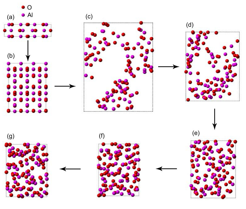 Figure 1
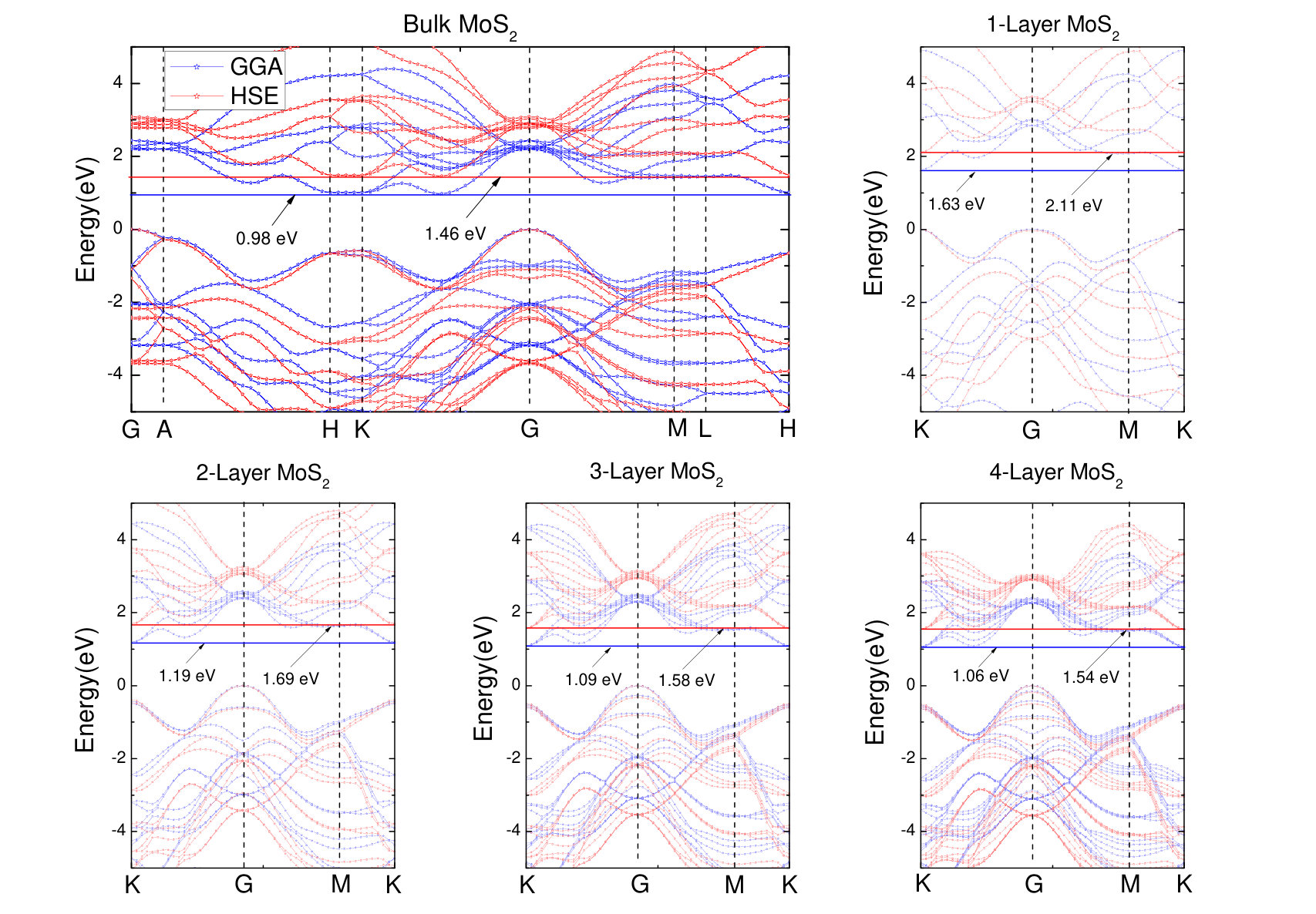 Figure 2
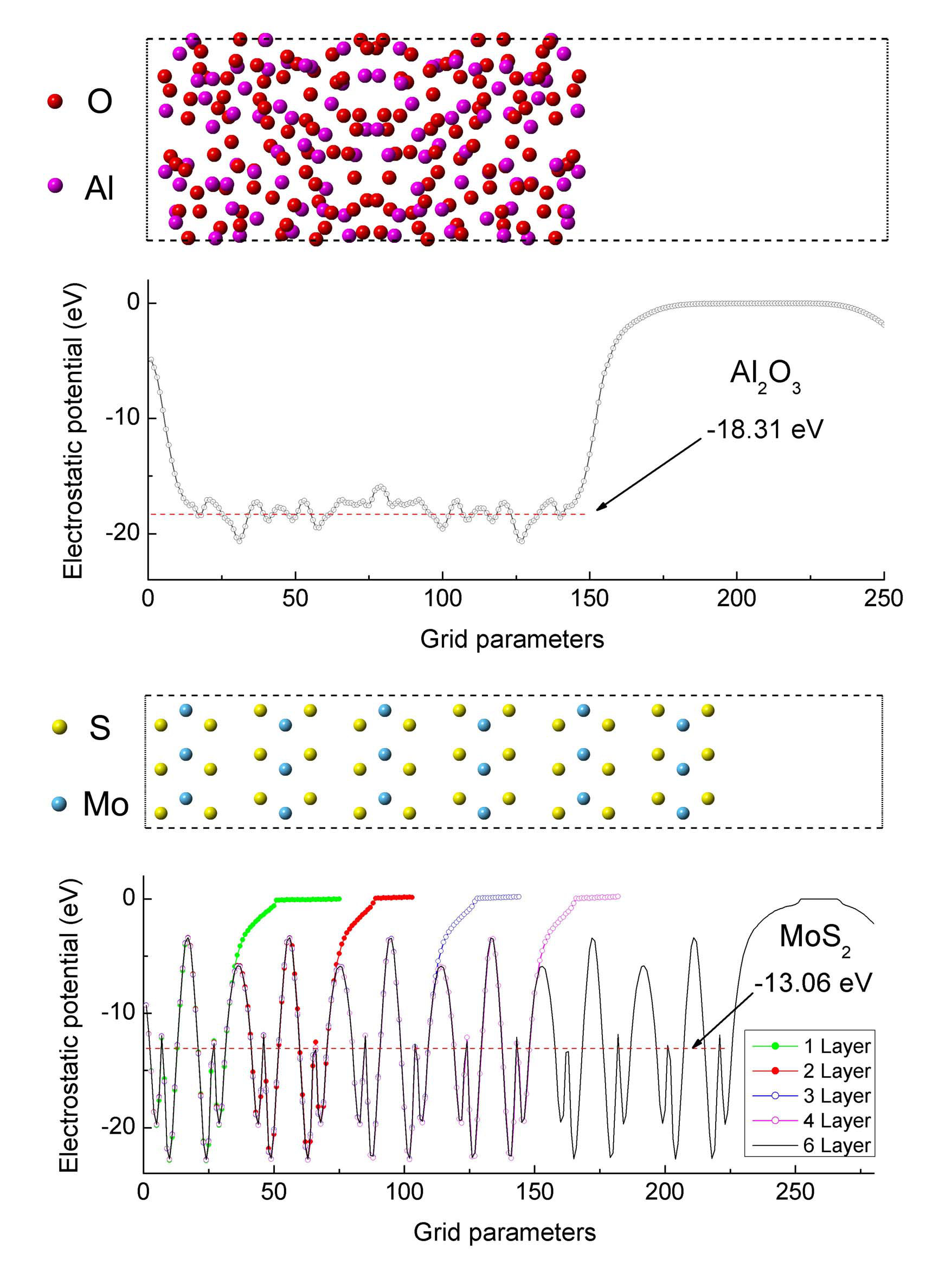 Figure 3
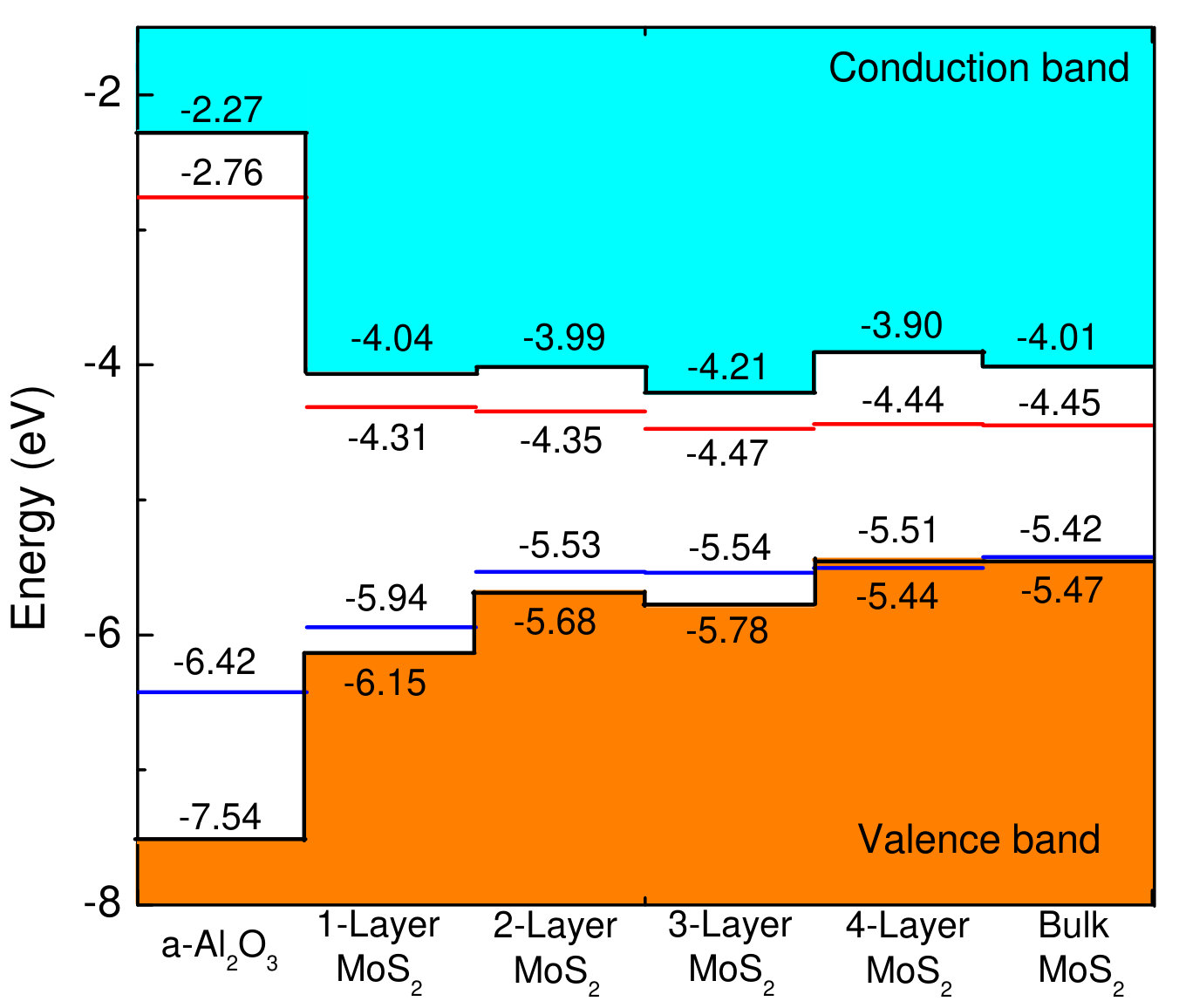 Figure 4
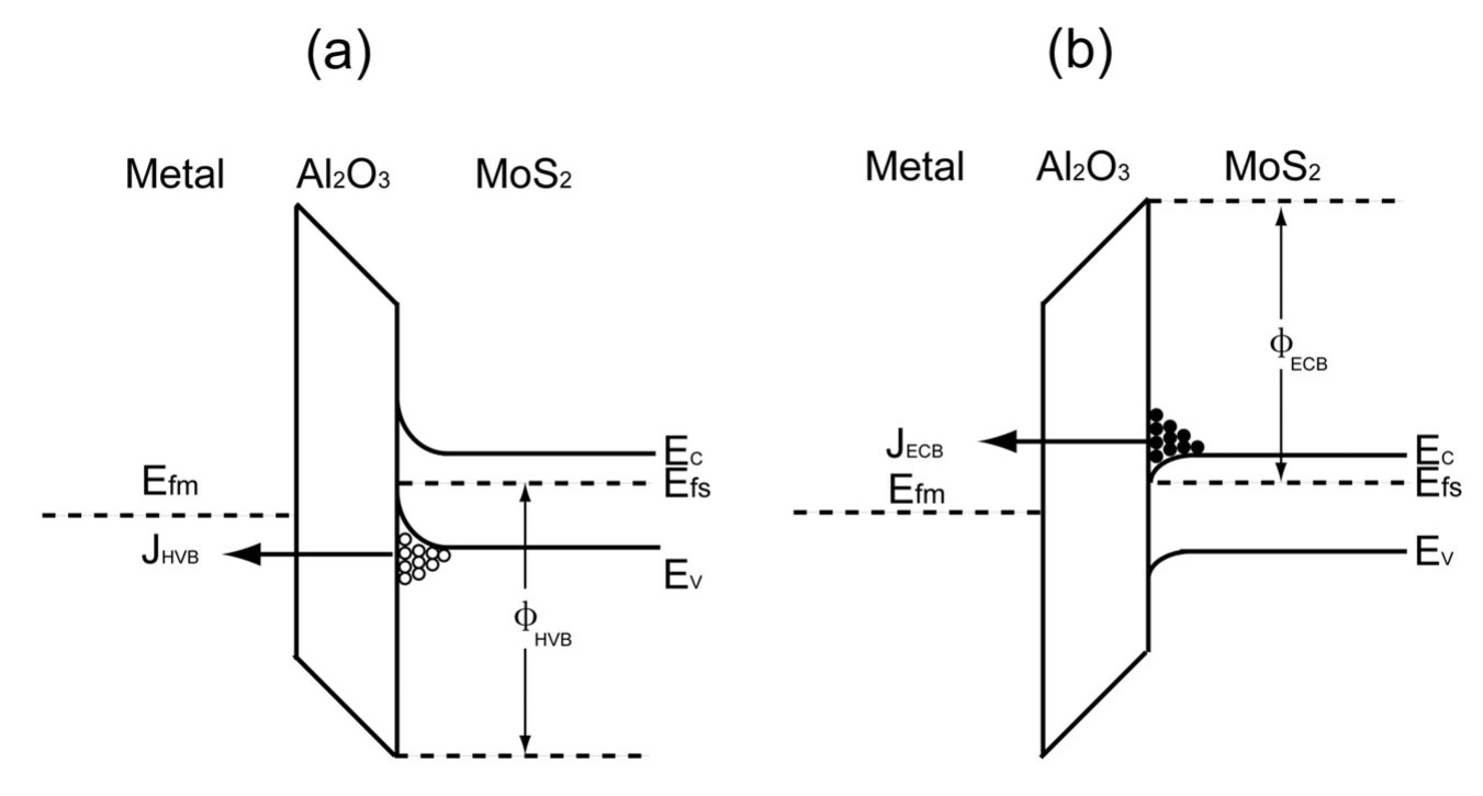 Figure 5
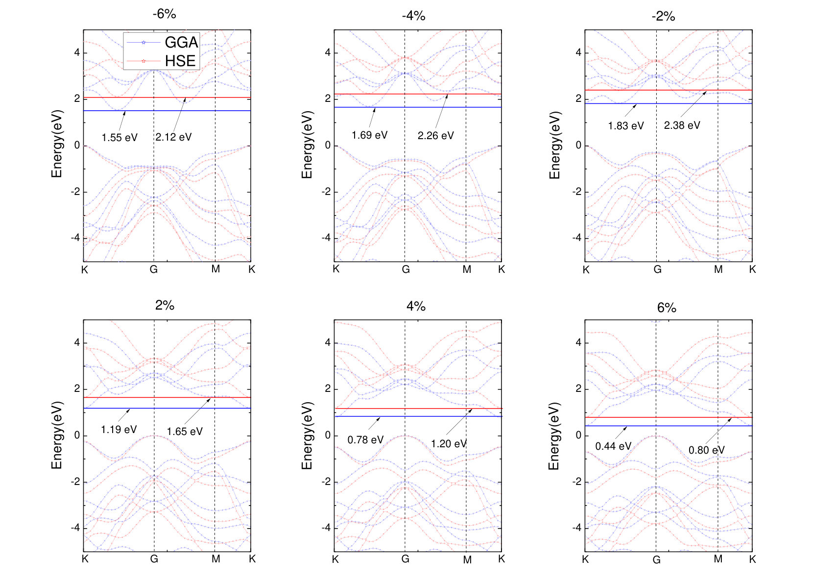 Figure 6
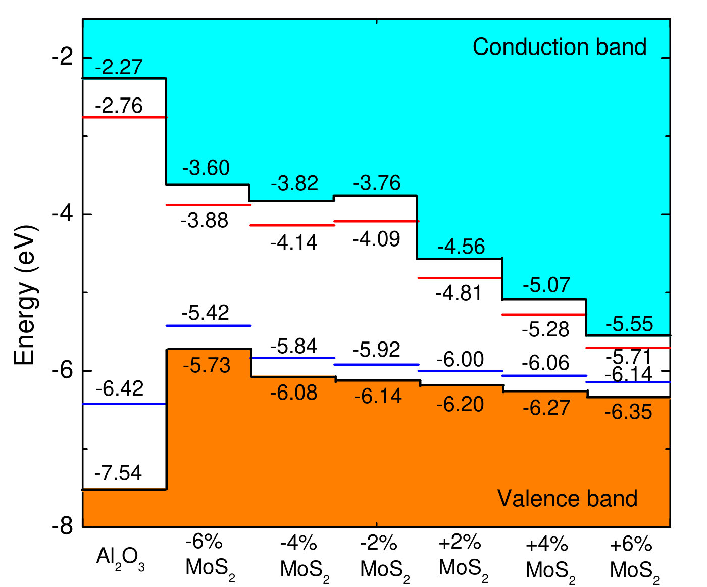 Figure 7
| Material | ||||
|---|---|---|---|---|
| 0.64 | 0.73 | 1.19 | 1.12 Afanas ev et al. (2006) | |
| 0.65 | 0.89 | 1.39 | 1.42 Windhorn et al. (1982) | |
| monolayer | 1.84 | 1.63 | 2.11 | 1.90 Mak et al. (2010) |
| bulk | 0.60 | 0.98 | 1.46 | 1.30 Mak et al. (2010) |
| 3.79 | 3.79 | 5.39 | 5.83 French et al. (1994) | |
| 4.52 | 4.67 | 6.17 | 5.80 He et al. (2007) | |
| 4.17 | 4.27 | 5.68 | 6.00 Ohta et al. (2004) | |
| 3.49 | 3.54 | 5.08 | 5.18 Qiya et al. (2014) | |
| 3.47 | 3.66 | 5.26 | 3.26.7Costina and Franchy (2001); Liu et al. (2012) | |
| 5.87 | 5.90 | 8.65 | 8.80 French (1990) | |
| 4.95 | 4.99 | 6.68 | ||
| 4.54 | 4.59 | 6.28 |
Peer Reviews
No public reviews on file for this paper yet. If you reviewed it on a platform where reviews are public (OpenReview, ICLR, NeurIPS, ICML), you can paste yours below so the community can read it here.
Videos
No videos yet. Explain this paper in a talk, walkthrough, or lecture? Add one.
First principles calculations of the interface properties of amorphous-/ under non-strain and biaxial strain conditions
Li-Bin Shi
[email protected]; [email protected]
Ming-Biao Li
Xiao-Ming Xiu
Xu-Yang Liu
Kai-Cheng Zhang
Yu-Hui Liu
Chun-Ran Li
Hai-Kuan Dong
School of Mathematics and Physics, Bohai University, Liaoning Jinzhou 121013, China
Abstract
is a potential dielectric material for metal-oxide-semiconductor (MOS) devices. films deposited on semiconductors usually exhibit amorphous due to lattice mismatch. Compared to two-dimensional graphene, is a typical semiconductor, therefore, it has more extensive application. The amorphous-/ (a-/) interface has attracted people’s attention because of its unique properties. In this paper, the interface behaviors of a-/ under non-strain and biaxial strain are investigated by first principles calculations based on density functional theory (DFT). First of all, the generation process of a- sample is described, which is calculated by molecular dynamics and geometric optimization. Then, we introduce the band alignment method, and calculate band offset of a-/ interface. It is found that the valence band offset (VBO) and conduction band offset (CBO) change with the number of layers. The dependence of leakage current on the band offset is also illustrated. At last, the band structure of monolayer under biaxial strain is discussed. The biaxial strain is set in the range from -6% to 6% with the interval of 2%. Impact of the biaxial strain on the band alignment is investigated.
pacs:
68.35.-p, 77.55.D-, 77.80.bn
I Introduction
Since integrated circuit was born in 1958, the microelectronic technology has made rapid development. Moore’s law predicts that the number of metal-oxide-semiconductor-field-effect-transistors (MOSFETs) on a chip doubles every 18 months.Moore (1998) For a long time, the gate oxide of integrated circuit has been using silicon dioxide. In order to further reduce the feature size of integrated circuits, we must abandon silicon dioxide, and select the materials with higher relative dielectric constant (high-).He et al. (2013, 2011) If high- materials are used to replace conventional silicon dioxide as the gate dielectric material, the physical thickness of the gate dielectric layer can be increased, so that the gate leakage current can be greatly suppressed. In order to develop field effect transistors with lower power consumption and higher efficiency, people have done a lot of research on high- materials, including ,Fang et al. (2012) ,Park et al. (1996) , Hong et al. (1999) , Chiu et al. (2005) ,Wu et al. (2015) ,Cai et al. (2007) ,Hsieh et al. (2008) , Xiong and Robertson (2009) ,Guo et al. (2013); Choi et al. (2013a); Hoex et al. (2008); Werner et al. (2011); Lin et al. (2013); Suh et al. (2013) , Liu et al. (2013a) ,Choi et al. (2007) ,Olyaei et al. (2012) ,Zheng et al. (2007) , Kang et al. (2003) Hf silicate,Xiong et al. (2007) and Zr silicate.Cota et al. (2013) among them has become a promising candidates due to its larger band gap (59 eV) and moderate dielectric constant (810).
thin films deposited on semiconductor substrates usually display amorphous due to lattice mismatch between and semiconductors. Costina and Franchy (2001); Liu et al. (2013b); Hu et al. (2014); Chagarov and Kummel (2008); Gutierrez and Johansson (2002); Lamparter and Kniep (1997) Amorphous- (a-) has a complex structure, and knowledge of its microstructure plays an important role in the analysis of the oxidation and passivation details of aluminum. A-/semiconductor interface is expected to be superior to crystalline-/semiconductor interface due to lower interface defect density. At present, a large number of theoretical and experimental studies have been done on crystalline ,Guo et al. (2013); Choi et al. (2013a); Hoex et al. (2008); Werner et al. (2011); Lin et al. (2013); Suh et al. (2013) which mainly include the crystal structure, defect formation and electronic structure. There is not much research on a- as a dielectric due to the complex microscopic structure. In particular, there is less theoretical research on the formation mechanism of a-.
Since the discovery of graphene in 2004, two-dimensional materials have attracted people’s attention.Novoselov et al. (2004); Nguyen and Hieu (2016); Lanzillo et al. (2016) Low dimensional materials are interesting not only because they can provide access to novel physical phenomena, but also because their unique electrical, optical and mechanical properties make them the focus of attention.Chang (2015); Chang et al. (2013); Banerjee et al. (2016); Nishiguchi et al. (2015); Kang et al. (2013) crystal is composed of Mo atomic layer sandwiched between two layers of S, forming a triangular prismatic arrangement.Han et al. (2011); Das et al. (2012) The Mo-S bonding is strong covalent, but the coupling between monolayer is weak van der Waals interactions. Because monolayer is a typical semiconductor, it is considered as promising candidates for nanoelectronics applications. However, one of the major limiting factors for low dimensional materials is the interface. At present, people have done some research on and .Singh et al. (2015); Son et al. (2015) However, the / interface properties are paid little attention. We have not found a detailed study of the a-/ interface under biaxial strain.
In this paper, we have done three aspects of studies. First, we investigate generation of a- by first principles molecular dynamics simulations. Then, we analyze band alignment between a- and . Impact of the layer thickness on band offset is discussed. At last, we investigate effects of the biaxial strain on a-/ interface. Impact of the band offset on leakage current is discussed.
II Computational details
II.1 Generation of amorphous- sample
Amorphous- is generated by melting and quenching technique. Molecular dynamics with NVT ensemble and geometric optimization based on density functional theory (DFT) are performed in the calculation. Generalized gradient approximation (GGA) of Perdew, Burke, and Ernzerhof (PBE) is choose as exchange correlation functional during molecular dynamics simulation.Perdew et al. (1996) All calculations are carried out in CASTEP code based on the total-energy pseudopotential method.Segall et al. (2002)
Figure 1 describes the specific generation process of a- sample. It is prepared by starting with a monoclinic crystal corresponding to - at the density of 3.61 , which is presented in Fig. 1 (a). Its lattice constants are a=11.80Å, b=2.91Å, and c=5.62Å. In order to perform molecular dynamics simulations, we cut - along (100) direction, and construct a orthogonal supercell by extension. The supercell consists of 72 O and 48 Al atoms with lattice constants of a=8.73Å, b=11.24Å, and c=11.50Å, which is shown in Fig. 1(b). High temperature annealing at low density provides very good oxide mixing and completely removes the original ordered geometry. The low density sample is formed by rescaling the supercell box size along every direction. In order to ensure the full mixing between the oxides, we construct the low density sample with value of 0.62 by expanding the supercell box size 1.8 times. Fig. 1 (c) presents the sample prepared by annealing at 5000 K for 1 ps with time step of 1 fs. In order to obtain experimental results, we must gradually increase the sample density. We first increase the sample density to 1.32 by rescaling the supercell box size from 1.8 times to 1.4 times, subsequent sample is annealed at 5000 K for 0.5 ps with time step of 1 fs. Fig. 1 (d) shows the sample after annealing at 5000 K. Then, the sample density is increased to 2.37 by rescaling the supercell box size from 1.4 times to 1.15 times. Fig. 1 (e) shows the sample annealed at 5000 K for 0.5 ps with time step of 1 fs. Finally, we increase the sample density to 3.4 by rescaling the supercell box size, which is in agreement with experimental values of 3.05 3.40 for a- sample Lee et al. (1995); Oka et al. (1979). The sample is annealed at 5000 K for 0.5 ps with time step of 1 fs, and quickly cooled up to 10 K. Fig. 1 (f) presents the cooled sample. In order to eliminate the internal stress, we do geometric optimization on samples, which is shown in Fig. 1 (g).
The electronic structure analysis for the annealed and relaxed a- indicates a band gap of 3.66 eV, which is in agreement with a previous DFT band gap of 3.80 eV.Chagarov and Kummel (2008) It is well known that the GGA underestimate band gaps of semiconductors or oxides, which leads to inaccurate calculations of band alignments. The hybrid Heyd-Scuseria-Ernzerhof functional (HSE) combines screened Hartree Fock exchange with the GGA-PBE Heyd et al. (2003); Heyd and Scuseria (2004); Paier et al. (2006); Heyd et al. (2005), which can give an accurate description on band gaps of semiconductors or oxides Lyons et al. (2011); De Walle et al. (2013); Choi et al. (2013b). Table 1 presents the band gaps of some semiconductors and oxides calculated by different exchange correlation functionals. The results indicate that the values calculated by HSE functional are close to the experiments. The a- band gap is increased to 5.26 eV by applying the HSE functional. The experimental values of a- band gap is in the range from 3.2 eV to 6.7 eV,Costina and Franchy (2001); Liu et al. (2012) which is closely related to the film growth technology. By comparison, we consider that the band gap value calculated by HSE functional is reasonable.
Table 2 presents averaged bond lengths of O-O, Al-O and Al-Al for our a- sample, which is compared with previous simulations and experiments. Our results are found to be very close to previous simulations and experiments, which indicates that our a- sample is close to the actual situation.
II.2 Band alignment methods
One of the most important features on oxide/semiconductor interfaces is band offset, i.e., the relative energy level positions on both sides of the interface. The valence band offset (VBO) can be defined as the difference between positions of valence band maximum (VBM), which can be obtained by calculating the band structure and average electrostatic potential (AEP). In the potential line up method, the VBO is usually split into two terms. Silvestri et al. (2013); D*′*Amico et al. (2012)
[TABLE]
The first contribution of corresponds to alignment of VBM for bulk band structure term of oxide and semiconductor. The second term of corresponds to the macroscopic AEP alignment, which can be determined by two methods. One method is to determine the macroscopic AEP by constructing the oxide/semiconductor interface. The other is to determine the macroscopic AEP by constructing oxide and semiconductor surfaces. / interface has been extensively investigated because the in-plane lattice mismatch between and along (001) direction is less than 3%. In order to verify the validity of two methods, we calculate the VBO by constructing and surfaces as well as / interface. It is found that the surface and interface calculations can give similar results, which is also found in previous investigation of /III-V interface Weber et al. (2011). The VBO calculated by constructing material surface is similar to that calculated by calculating the work function of the material, which has been widely used to study the band offset. Liu et al. (2007); Kang et al. (2013)
In this paper, we align the macroscopic AEP by constructing a- and surfaces instead of a-/ interface. The reasons are as follows. (a) There is a large difference in the atomic arrangement of a- and . The atoms near interface can only reach equilibrium state through larger migration. The atomic migration causes the AEP distortion, which lead to a inaccurate alignment of macroscopic AEP. However, this problem can be avoided by a- and surfaces. (b) The interface structure will produce a larger cell, which takes more time to calculate. Especially for the nonlocal HSE calculation, the cell size will have a great influence on the calculation time.
A- surface contains 144 O and 96 Al atoms. In order to avoid the interaction between the top and bottom layer, a vacuum region of 16 Å is built to separate them. surface containing layer number from 1 to 6 is built, which has a vacuum region of 16 Å. The monolayer surface contains 18 S and 9 Mo atoms. The cores for all atoms are represented by norm-conserving pseudopotential, while the valences states are expanded in a plane-wave basis set with 600 eV.
III Results and discussion
III.1 Band alignment of a-/ interface
In order to elucidate band gap shift, we calculate the band structures for bulk and different thickness layers of by GGA-PBE and HSE functionals as shown in Fig. 2. The band structures suggest that bulk is a semiconductor with indirect band gap, the VBM at G-point, and the conduction band minimum (CBM) between K-point and G-point. This calculation is consistent with previous investigation.Han et al. (2011) Calculated band gap is 0.98 eV for GGA-PBE and 1.46 eV for HSE. It is found that HSE band gap is close to experimental value of 1.30 eV.Mak et al. (2010) For 4-layer , the band gap is increased to 1.06 eV for GGA-PBE and 1.54 eV for HSE. We are surprised to find that the CBM shifts to K-point as changes from bulk structure to 4-layer . However, the positions of VBM can not be found to change significantly. It is noted that the band gap increases with the decrease of the number of layers. The GGA-PBE and HSE band gaps are increase to 1.09 eV and 1.58 eV for 3-layer , and 1.19 eV and 1.69 eV for 2-layer . Interestingly, the position of VBM shifts from G-point to K-point as changes from 2-layer to 1-layer (monolayer ). Therefore, it changes from indirect gap semiconductor to direct band gap semiconductor. The GGA-PBE and HSE band gaps are increase to 1.63 eV and 2.11 eV for 1-layer . The experimental value of band gap for monolayer is 1.90 eV.Mak et al. (2010) Comparing to the experimental values, it is found that the band gap is underestimated by GGA-PBE while it is slightly overestimated by HSE.
Figure 3 shows a- and surfaces as well as planar and macroscopic AEP. In order to align the AEP, the vacuum level is scaled to zero. Macroscopic AEP is the averaged value of planar AEP, which is represented by a red point connection in Fig. 03. For surface, the planar AEP in the atomic region exhibits a periodic oscillation, while it remains constant in the vacuum region.Shi et al. (2016) It is found that the shape of planar AEP do not change as the number of the layers changes from 1 to 6. For a- surface, the planar AEP in the atomic region has no obvious periodicity. The value of macroscopic AEP for surface is -13.06 eV while its values is -18.31 eV for a-.
Figure 4 shows band alignment between a- and . In the following, we discuss the VBO and CBO at a-/ interface in Fig. 04 based on HSE and GGA-PBE calculations. The VBO and CBO based on HSE calculations are 1.39 eV and 1.77 eV for 1-layer , 1.86 eV and 1.72 eV for 2-layer , 1.76 eV and 1.94 eV for 3-layer , 2.10 eV and 1.63 eV for 4-layer , and 2.07 eV and 1.74 eV for bulk . Previous investigations have indicated that VBO and CBO can be affected by the thickness of .Nishiguchi et al. (2015) The VBO and CBO based on GGA-PBE calculations are 0.48 eV and 1.55 eV for 1-layer , 0.89 eV and 1.59 eV for 2-layer , 0.88 eV and 1.71 eV for 3-layer , 0.91 eV and 1.68 eV for 4-layer , and 1.00 eV and 1.69 eV for bulk . GGA-PBE underestimates the band gap, which leads to inaccurate VBO and CBO.Lin et al. (2013); Yang et al. (2014) The VBM and CBM positions of a- and are shown in Fig. 04. The VBM position of monolayer is -5.94 eV for GGA-PBE, and -6.15 eV for HSE, which is close to previous results of -5.87 eV and -6.27 eV.Kang et al. (2013) It is noted that VBM position moves upward as the number of layers is increased.
Figure 5 exhibits energy band diagrams for metal/a-/n-type MOS under negative and positive voltages. The energy band near will bend upwards as the negative voltage is applied between the metal and .Yeo et al. (2000) The surface layer changes from the majority carrier depletion to the minority carrier inversion with the increase of the voltage. In this case, the hole tunneling barrier of is determined by VBO. Leakage current is expressed as . The energy band near will bend down as the positive voltage is applied to devices. The surface layer is in majority carrier accumulation region with the increase of the positive voltage. In this case, the electron tunneling barrier of is determined by CBO. The leakage current is written as . Similar analysis is also suitable for metal/a-/p-type MOS. In our model, the carrier tunneling current is closely related to the VBO and CBO. The band offset is sensitive to thickness of , which affects the leakage current of the device to a certain extent. At present, it is generally believed that VBO or CBO in ideal MOS device should be greater than 1 eV.Das et al. (2010); Hong et al. (1999); Van de Walle et al. (2013); Sun et al. (2008a, b, 2007) It is noted that the VBO or CBO calculated by HSE for different thickness is greater than 1 eV. Therefore, we believe that metal/a-/ MOS can be an ideal device.
III.2 Impact of biaxial strain on the band alignment
The biaxial strain of monolayer is defined as ,Kaloni et al. (2013) where and are lattice constants of strained and non strained . and corresponds to the tensile and compressive strain, respectively. Strain engineering may improve physical performances of semiconductors, in particular, their transport properties.Liu et al. (2015a); Yu et al. (2015); Chang et al. (2015); Zhang et al. (2009); Fiori et al. (2013); Cheng et al. (2013); Chern et al. (2014) This inspires us to study the effect of biaxial strain on monolayer . The lattice strain is set in the range from -6% to 6% with the interval of 2%. Figure 6 presents the band structures for monolayer under biaxial strain. The monolayer is change to be a indirect band gap semiconductor under biaxial compressive strain, the VBM at K-point, and the CBM between K-point and G-point. The band gaps of GGA and HSE are increased to 1.83 eV and 2.38 eV for -2%, 1.69 eV and 2.26 eV for -4%, and 1.55 eV and 2.12 eV for -6%. The band gap first achieves the maximum value at =-2%, and then gradually decreases with biaxial compressive strain. Similar results are also found on GaAs.Shi et al. (2017) The band structures of HSE are similar in shape with GGA-PBE, and the band gap values are increased by HSE functional. Interestingly, under biaxial tensile strain, the position of VBM shifts to G-point, and the CBM to K-point. The band gaps are decreased to 1.19 eV and 1.65 eV for 2%, 0.78 eV and 1.20 eV for 4%, 0.44 eV and 0.80 eV for 6%. It is noted that band gaps for monolayer will decrease with biaxial tensile strain, which is in agreement with previous investigation. Nguyen and Hieu (2016); Lanzillo et al. (2016)
Figure 7 presents band alignment for a-/monolayer interface under biaxial strain. The VBM and CBM position of a- and monolayer are shown in Fig. 7. The VBM of monolayer consists of , orbits of Mo and , orbits of S.Liu et al. (2015b) Its position originates from the repulsion between , orbits of Mo and , orbits of S. The CBM of monolayer consists of orbit of Mo and , orbits of S. Its position originates from the repulsion between orbit of Mo and , orbits of S. This repulsion is closely related to the overlap of the d orbits of Mo and p orbits of S, and their difference in energy. The overlap is gradually weakened as the biaxial strain changes from -6% to 6%. Therefore, the VBM and CBM of monolayer move downward as the strain changes from compressive strain to tensile strain. For GGA-PBE calculations, the VBO and CBO are 1.00 and 1.12 eV for =-6%, 0.58 and 1.38 eV for =-4%, 0.50 and 1.33 eV for =-2%, 0.42 and 2.05 eV for =2%, 0.36 and 2.52 eV for =4%, 0.28 and 2.95 eV for =6%. For HSE calculations, the VBO and CBO are increased to 1.81 and 1.33 eV for =-6%, 1.46 and 1.55 eV for =-4%, 1.40 and 1.49 eV for =-2%, 1.34 and 2.29 eV for =2%, 1.27 and 2.80 eV for =4%, 1.19 and 3.28 eV for =6%. It is found from the results that the appropriate biaxial tensile strain in monolayer can increase the CBO, while the change of VBO is smaller, which effectively suppresses leakage current of the devices. Previously, Tabatabaei et al. Mohammad Tabatabaei et al. (2013) have found that performance of field effect transistor can be improved significantly by biaxial strain, which is consistent with the our investigation.
IV Conclusions
The generation process of amorphous- sample is described by molecular dynamics and geometric optimization. The averaged bond lengths of O-O, Al-O and Al-Al for our amorphous- sample are agreement with previous simulations and experiments. The results show that our sample is close to the actual situation.
The band alignment of oxide and semiconductor can be obtained by building both surface and interface methods. We have verified the results by building / interface. It is found that the surface and interface calculations can give similar results.
In order to avoid the waste of calculation time and AEP distortion, we realize band alignment of amorphous-/ by building both amorphous- and surfaces. For HSE calculations, the VBO and CBO are 1.39 eV and 1.77 eV for 1-layer , 1.86 eV and 1.72 eV for 2-layer , 1.76 eV and 1.94 eV for 3-layer , 2.10 eV and 1.63 eV for 4-layer , and 2.07 eV and 1.74 eV for bulk . The VBO and CBO can be changed by the thickness because the band gap of is sensitive to its thickness. The effect of VBO and CBO on the leakage current is also analyzed.
The VBO and CBO based on HSE calculation are increased to 1.81 and 1.33 eV for =-6%, 1.46 and 1.55 eV for =-4%, 1.40 and 1.49 eV for =-2%, 1.34 and 2.29 eV for =2%, 1.27 and 2.80 eV for =4%, 1.19 and 3.28 eV for =6%. The positions of VBM and CBM for monolayer move downward as the strain changes from =-6% to =6%. It is noted that the VBO and CBO are larger than 1 eV, indicating that metal/amorphous-/ is an ideal MOS device.
Acknowledgements.
The work is supported by the National Natural Science Foundation of China under Grant No. 11547182 and No. 11674037.
The reference list from the paper itself. Each links out to its DOI / PubMed record.
- 1Moore (1998) G. E. Moore, Proceedings of the IEEE 86 , 82 (1998).
- 2He et al. (2013) G. He, X. Chen, and Z. Sun, Surface Science Reports 68 , 68 (2013).
- 3He et al. (2011) G. He, L. Zhu, Z. Sun, Q. Wan, and L. Zhang, Progress in Materials Science 56 , 475 (2011).
- 4Fang et al. (2012) Q. F. Fang, C. Hodson, M. Liu, Z. W. Fang, R. Potter, and R. Gunn, Physics Procedia 32 , 379 (2012).
- 5Park et al. (1996) D.-G. Park, D. M. Diatezua, Z. Chen, S. N. Mohammad, and H. Morkoç, Applied physics letters 69 , 3025 (1996).
- 6Hong et al. (1999) M. Hong, J. Kwo, A. Kortan, J. Mannaerts, and A. Sergent, Science 283 , 1897 (1999).
- 7Chiu et al. (2005) F. C. Chiu, H. W. Chou, and J. Y. Lee, Journal of Applied Physics 97 , 103503 (2005).
- 8Wu et al. (2015) S. Wu, K. Chen, Y. Lin, C. Cheng, C. Hsu, J. Kwo, and M. Hong, Microelectronic Engineering 147 , 310 (2015).