Out-of-plane heat transfer in van der Waals stacks: electron-hyperbolic phonon coupling
K. J. Tielrooij, N. C. H. Hesp, A. Principi, M. Lundeberg, E. A. A., Pogna, L. Banszerus, Z. Mics, M. Massicotte, P. Schmidt, D. Davydovskaya, D., G. Purdie, I. Goykhman, G. Soavi, A. Lombardo, K. Watanabe, T. Taniguchi, M., Bonn, D. Turchinovich, C. Stampfer, A. C. Ferrari

TL;DR
This paper uncovers an efficient out-of-plane heat transfer mechanism in van der Waals heterostructures, where charge carriers couple to hyperbolic phonon polaritons, enabling ultrafast cooling and potential heat flow control.
Contribution
It demonstrates a novel hyperbolic phonon polariton-mediated heat transfer process in van der Waals stacks, validated by theory and experiments with no adjustable parameters.
Findings
Hyperbolic phonon polaritons enable ultrafast picosecond cooling.
Heat transfer efficiency depends on carrier density and temperature.
Excellent agreement between experimental results and theoretical predictions.
Abstract
Van der Waals heterostructures have emerged as promising building blocks that offer access to new physics, novel device functionalities, and superior electrical and optoelectronic properties. Applications such as thermal management, photodetection, light emission, data communication, high-speed electronics and light harvesting require a thorough understanding of (nanoscale) heat flow. Here, using time-resolved photocurrent measurements we identify an efficient out-of-plane energy transfer channel, where charge carriers in graphene couple to hyperbolic phonon polaritons in the encapsulating layered material. This hyperbolic cooling is particularly efficient, giving picosecond cooling times, for hexagonal BN, where the high-momentum hyperbolic phonon polaritons enable efficient near-field energy transfer. We study this heat transfer mechanism through distinct control knobs to vary carrier…
Click any figure to enlarge with its caption.
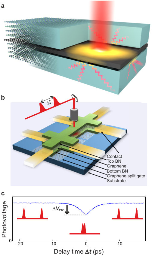 Figure 1
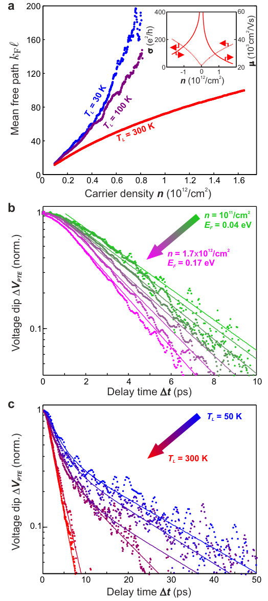 Figure 2
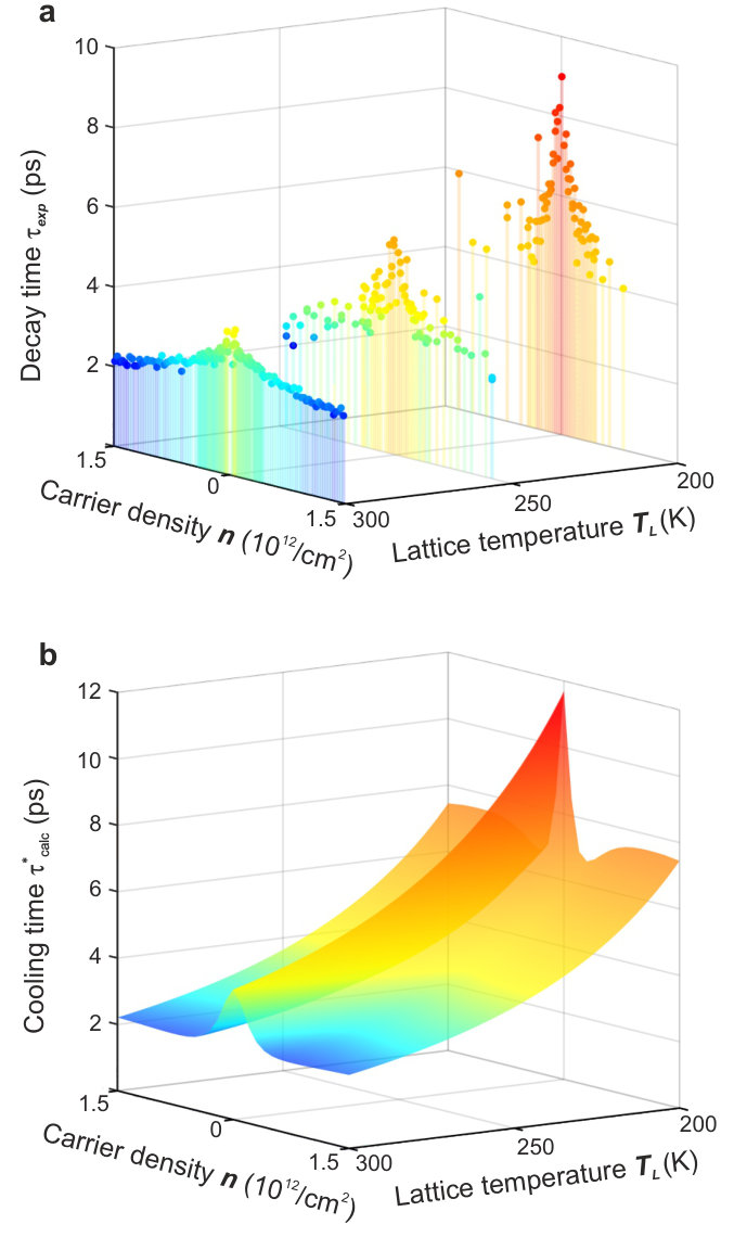 Figure 3
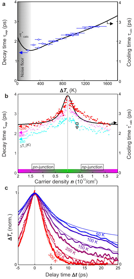 Figure 4
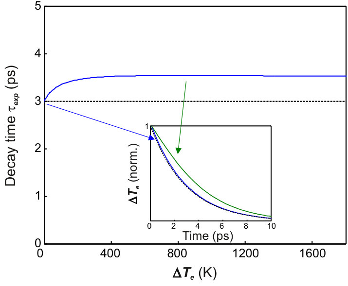 Figure 1
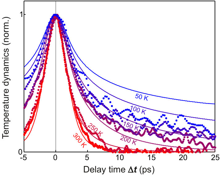 Figure 10
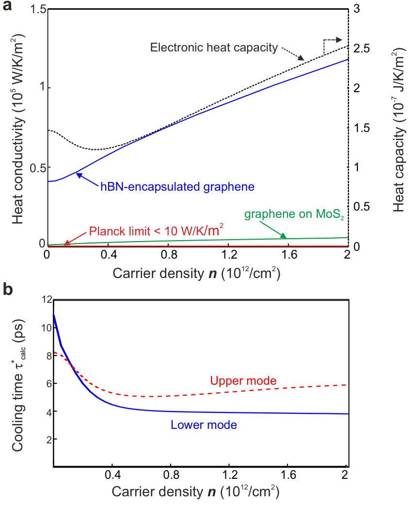 Figure 11
 Figure 3
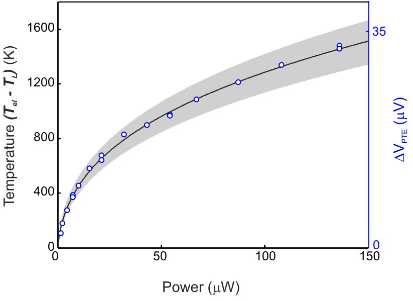 Figure 4
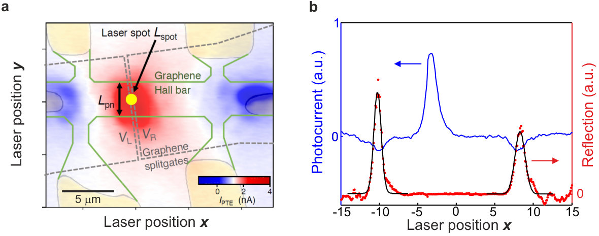 Figure 5
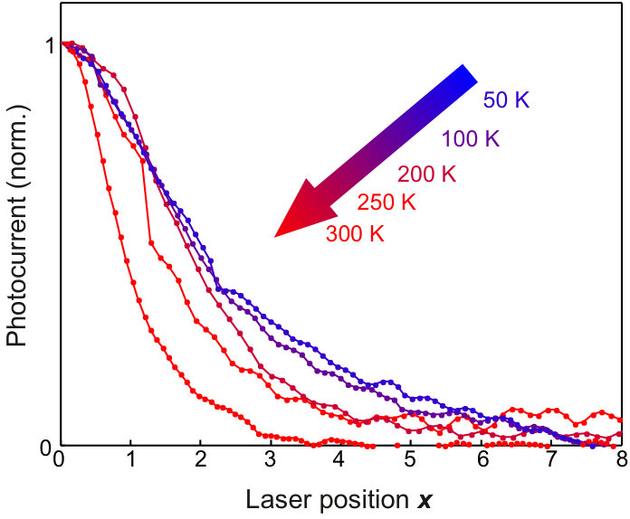 Figure 6
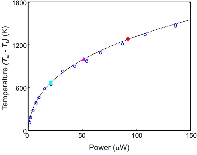 Figure 7
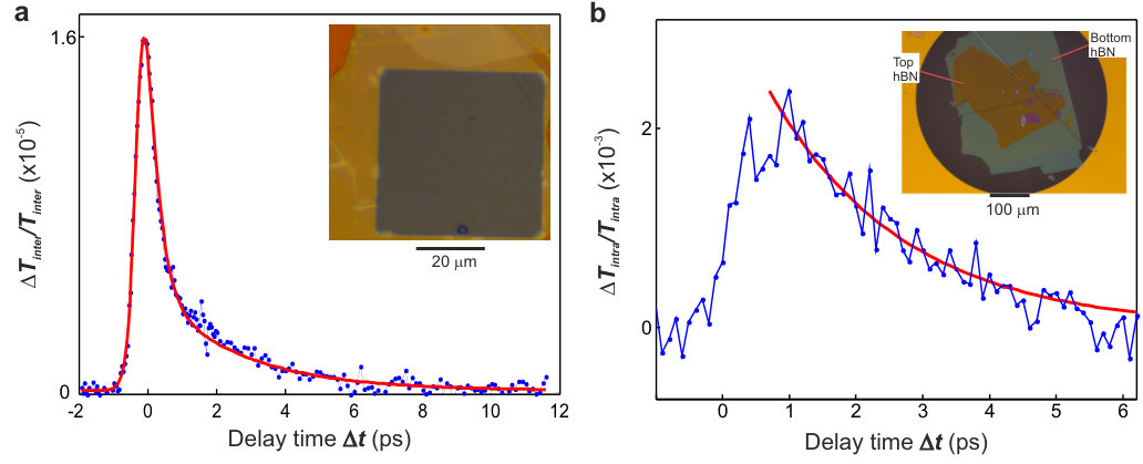 Figure 8
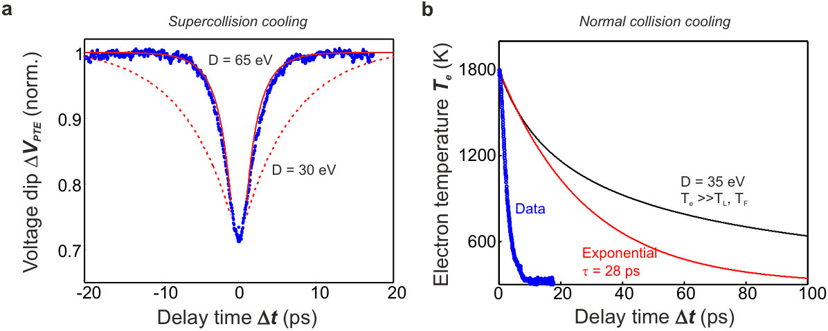 Figure 9
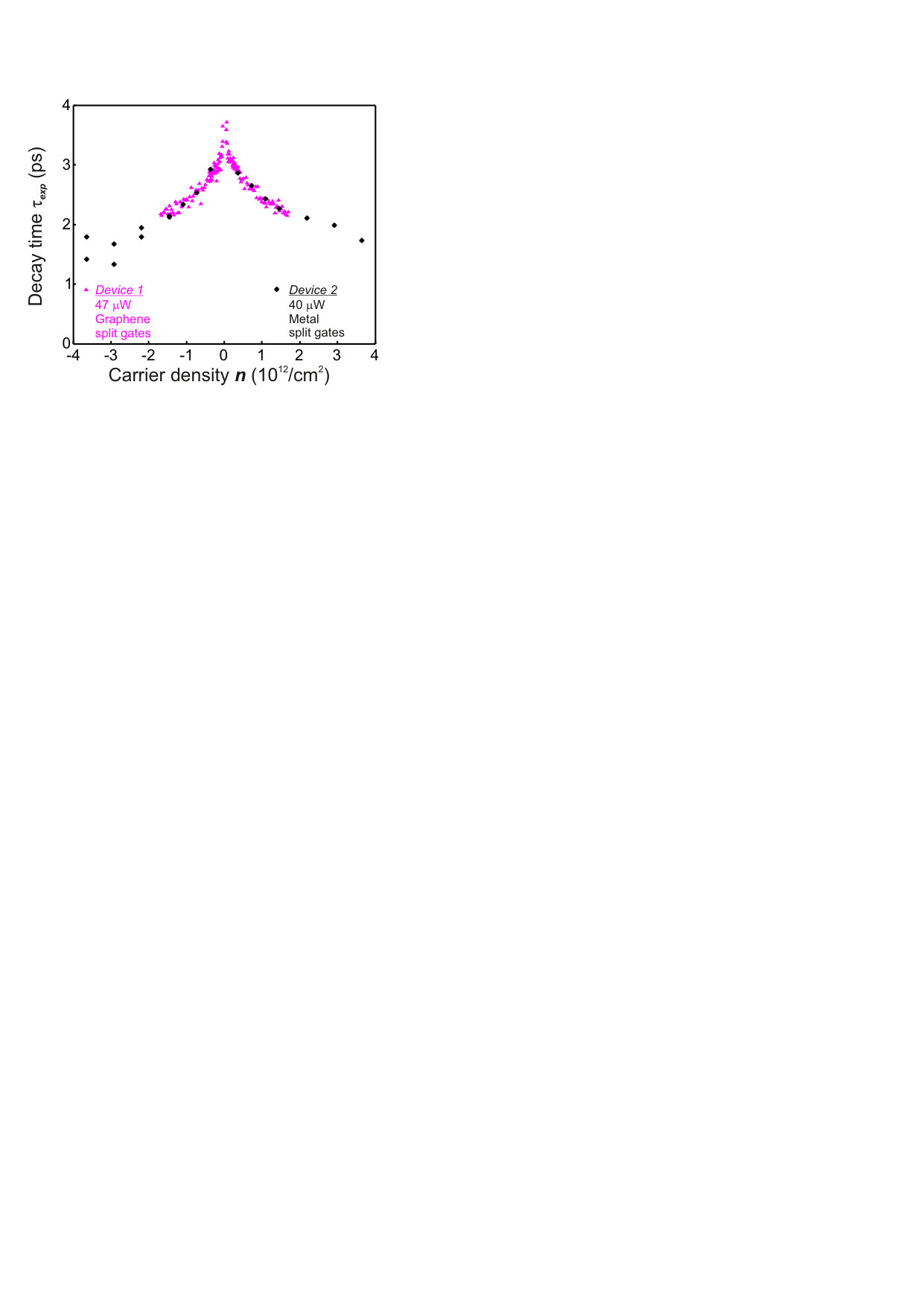 Figure 15
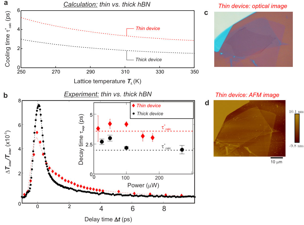 Figure 16
Peer Reviews
No public reviews on file for this paper yet. If you reviewed it on a platform where reviews are public (OpenReview, ICLR, NeurIPS, ICML), you can paste yours below so the community can read it here.
Videos
No videos yet. Explain this paper in a talk, walkthrough, or lecture? Add one.
Out-of-plane heat transfer in van der Waals stacks through electron-hyperbolic phonon coupling
Klaas-Jan Tielrooij,
Correspondence: [email protected], [email protected]
Niels C. H. Hesp,
ICFO - Institut de Ciències Fotòniques, The Barcelona Institute of Science and Technology, Castelldefels (Barcelona) 08860, Spain
Alessandro Principi
Radboud University, Institute for Molecules and Materials, NL-6525 AJ Nijmegen, the Netherlands
Mark B. Lundeberg
ICFO - Institut de Ciències Fotòniques, The Barcelona Institute of Science and Technology, Castelldefels (Barcelona) 08860, Spain
Eva A. A. Pogna
IFN-CNR, Dipartimento di Fisica, Politecnico di Milano, Piazza L. da Vinci 32, 20133 Milano, Italy
Luca Banszerus
JARA-FIT and 2nd Institute of Physics, RWTH Aachen University, 52074 Aachen, Germany
Zoltán Mics
Max Planck Institute for Polymer Research, Ackermannweg 10, Mainz 55128, Germany
Mathieu Massicotte
Peter Schmidt
Diana Davydovskaya
ICFO - Institut de Ciències Fotòniques, The Barcelona Institute of Science and Technology, Castelldefels (Barcelona) 08860, Spain
David G. Purdie
Ilya Goykhman
Giancarlo Soavi
Antonio Lombardo
Cambridge Graphene Centre, University of Cambridge, Cambridge CB3 OFA, UK
Kenji Watanabe
Takashi Taniguchi
National Institute for Material Science, 1-1 Namiki, Tsukuba 305-0044, Japan
Mischa Bonn
Dmitry Turchinovich
Max Planck Institute for Polymer Research, Ackermannweg 10, Mainz 55128, Germany
Christoph Stampfer
JARA-FIT and 2nd Institute of Physics, RWTH Aachen University, 52074 Aachen, Germany
Andrea C. Ferrari
Cambridge Graphene Centre, University of Cambridge, Cambridge CB3 OFA, UK
Giulio Cerullo
IFN-CNR, Dipartimento di Fisica, Politecnico di Milano, Piazza L. da Vinci 32, 20133 Milano, Italy
Marco Polini
Istituto Italiano di Tecnologia, Graphene Labs, Via Morego 30, I-16163 Genova, Italy
Frank H. L. Koppens
Correspondence: [email protected], [email protected]
ICFO - Institut de Ciències Fotòniques, The Barcelona Institute of Science and Technology, Castelldefels (Barcelona) 08860, Spain
ICREA - Institució Catalana de Reçerca i Estudis Avancats, 08010 Barcelona, Spain
Abstract
Van der Waals heterostructures have emerged as promising building blocks that offer access to new physics, novel device functionalities, and superior electrical and optoelectronic properties Geim2013 ; Dean2010 ; Mayorov2011 ; Britnell2012 ; Wang2013 ; Dean2013 ; Nanoscale15 . Applications such as thermal management, photodetection, light emission, data communication, high-speed electronics and light harvesting Balandin2008 ; Britnell2013 ; Koppens2014 ; Lopez2014 ; Bonaccorso2015 ; Mics2015 ; Kim2015 ; Massicotte2016 ; BonaNP10 require a thorough understanding of (nanoscale) heat flow. Here, using time-resolved photocurrent measurements we identify an efficient out-of-plane energy transfer channel, where charge carriers in graphene couple to hyperbolic phonon polaritons Caldwell2014 ; Dai2014 ; Basov2016 in the encapsulating layered material. This hyperbolic cooling is particularly efficient, giving picosecond cooling times, for hexagonal BN, where the high-momentum hyperbolic phonon polaritons enable efficient near-field energy transfer. We study this heat transfer mechanism through distinct control knobs to vary carrier density and lattice temperature, and find excellent agreement with theory without any adjustable parameters. These insights may lead to the ability to control heat flow in van der Waals heterostructures.
Owing to its large in-plane thermal conductivity, graphene has been suggested as material for the thermal management of nanoscale devices Balandin2008 . At the same time, graphene is well-known for its ability to convert incident light into electrical heat, i.e. hot electrons that can be used to generate photocurrent, with applications in photodetection, data communication and light harvesting Song2011 ; Gabor2011 ; Koppens2014 . Understanding, and ultimately controlling, heat flow in graphene-van der Waals heterostructures is therefore of paramount importance. For example, a short cooling time of graphene hot carriers is advantageous for thermal management and for high switching rates of photodetectors (PDs) for data communication, whereas a long cooling time is favorable for photodetection sensitivity Song2011 ; Gabor2011 ; Koppens2014 . Of particular relevance are heterostructure devices that contain high-quality graphene encapsulated by layered materials, such as hexagonal BN (hBN) and MoS2, which have the potential to crucially improve the performance of electronic and optoelectronic devices Dean2010 ; Geim2013 . †† Equal contribution.
A number of cooling pathways for graphene carriers have been proposed, involving among others strongly coupled optical phonons Kampfrath2005 ; Mihnev2016 ; Brida2013 , acoustic phonons Bistritzer2009 ; Song2012 ; Graham2013 ; Betz2013 , substrate phonons Low2012 and plasmons Hamm2016 (see also Appendix 1). Here, using several experimental approaches, we show that cooling in graphene encapsulated by hBN is governed by out-of-plane coupling of graphene electrons to special polar phonon modes that occur in layered materials (LMs): hyperbolic phonon polaritons, where 0, with and the permittivity parallel and perpendicular to the LM plane. Owing to this property, these materials carry deep sub-wavelength, ray-like optical phonon polaritons. For hBN, within the two Reststrahlen bands a large number of hyperbolic phonon modes exist with high momenta, far outside the light cone. The most notable modes occur at an energy of 100 meV and 180 meV Caldwell2014 , such that energy overlap with the graphene hot-carrier distribution is substantial. The unusual hyperbolic character gives rise to a very high density of optical states, and thus large thermal energy densities Caldwell2014 ; Dai2014 , thereby providing a potentially efficient cooling pathway for hot carriers in graphene. By near-field coupling between graphene and hBN, efficient energy transfer from hot carriers to hyperbolic phonon polaritons is possible Principi2016 . Here we show that the measured carrier dynamics of hBN-encapsulated graphene can be explained by this hyperbolic cooling process, as illustrated in Fig. 1****a.
We use ultrafast time-resolved photocurrent measurements and show the results obtained from one hBN-encapsulated, Hall-bar shaped, exfoliated graphene device (see Fig. 1****b). The device contains chemical vapor deposited (CVD) graphene split gates underneath the bottom hBN (thickness: 70 nm), in order to generate a -junction in the middle of the device. A second hBN-encapsulated device with metallic split gates gave fully consistent results. With 800 nm light incident on the -junction, a photovoltage is generated by the photo-thermoelectric (PTE) effect Song2011 ; Gabor2011 (see the photocurrent and reflection data in Fig. 5 and the characteristic PTE sixfold pattern in Fig. 6). By varying the delay between two sub-picosecond pulses we extract the carrier dynamics from the photovoltage signal (see Fig. 1****c). Since the photo-thermoelectric voltage scales with the light-induced increase in carrier temperature, the decay dynamics of closely mimic the cooling dynamics of the hot electron system (see Fig. 7 for an analysis of the extent to which the experimentally observed decay dynamics correspond to the underlying cooling dynamics). In the case of exponential decay dynamics, which we observe above a lattice temperature of 200 K, we extract an experimental cooling time scale by describing the decay dynamics with .
First, we electrically characterize our device using four-probe measurements (see Fig. 2****a) and find a mean free path of = 80–100 at a carrier density of /cm2, corresponding to a mobility of 25,000–30,000 cm2/Vs and momentum scattering time of 340–440 fs. As expected, this is much higher than SiO2-supported devices with typically 10, mobility 5,000 cm2/Vs and momentum scattering time 100 fs (see e.g. Ref. Graham2013 ). In such devices, carrier cooling is typically ascribed to disorder-assisted cooling to graphene acoustic phonons Song2012 ; Graham2013 ; Betz2013 .
To study hot-carrier cooling in our high-mobility, encapsulated devices we examine while varying graphene’s most characteristic parameter, the carrier density . In particular, we apply a gate voltage to the left split gate and to the right gate, such that there is always either a -junction or an -junction, with equal electron and hole densities in the two graphene regions ( is the gate voltage that corresponds to the Dirac point). The incident laser fluence is typically 5 – 40 J/cm2. The data show that cooling becomes faster upon increasing the carrier density (see Fig. 2****b). We also vary the lattice temperature and observe faster decay for increasing lattice temperature (see Fig. 2****c, taken at 1012/cm2). At low temperatures (below 200 K), cooling is non-exponential, whereas at room temperature we observe exponential decay of the photovoltage dip, with a timescale of 2.5 ps (for /cm2). We independently verify this cooling time using two alternative measurement techniques that are both sensitive to electron cooling dynamics in different ways (see Fig. 8). Firstly, using ultrafast optical pump – optical probe spectroscopy, which probes interband transitions Brida2013 , we find = 2.55 ps for the decay of the absorption photobleaching. Secondly, using optical pump – terahertz probe spectroscopy, which probes intraband transitions Mics2015 , we obtain = 2.2 ps for the decay of the photoconductivity. For these two experiments we use similar excitation conditions (an incident pulse fluence of 8–20 J/cm2) as in the photocurrent measurements, and the measurements are performed on two separate devices consisting of large-area, high-quality hBN-encapsulated CVD graphene as in Ref. Banszerus2015 . Thus, all three techniques consistently yield similar cooling times for hBN-encapsulated graphene.
We compare these observations with different cooling mechanisms, and note that the data are qualitatively and quantitatively inconsistent with in-plane cooling by scattering with graphene acoustic phonons through normal Bistritzer2009 or disorder-assisted collisions Song2012 ; Graham2013 ; Betz2013 (see Appendix 1 and Fig. 9). In-plane cooling can also occur by scattering to graphene optical phonons, typically occurring on a sub-picosecond timescale Kampfrath2005 ; Brida2013 . Reference Mihnev2016 reports that for non-encapsulated graphene this channel gives picosecond decay dynamics of the THz photoconductivity. However these results deviate in several ways from our observations for hBN-encapsulated graphene (see Appendix 1). For example, we observe a twofold increase in cooling time by decreasing from 300 K to 200 K, whereas optical phonon cooling gives cooling dynamics that are independent of substrate temperature (for = 0.3 eV), see Ref. Mihnev2016 . This indicates that, besides a fraction of hot graphene electrons possibly cooling through optical phonons, a different cooling mechanism plays an important role. Since we observe a striking effect of the hBN crystal slab thickness on the cooling dynamics (see Fig. 10 and Appendix 2), we propose an out-of-plane cooling mechanism where hot carriers in graphene lose their energy to remote polar phonons in the encapsulating layered material. The energy transfer can be understood from fluctuation electrodynamics, where any process that dissipates energy in the form of heat, has a reverse process that is driven by thermal fluctuations and thus becomes stronger at higher temperatures Nyquist1928 ; Mihnev2015 . An example of such paired processes is light absorption and blackbody radiation, which means that graphene emits thermal noise due to the dissipative real part (indicated by ) of the frequency- and momentum-dependent optical sheet conductivity . This thermal noise is efficiently absorbed by hBN, hBN being a lossy-polarizable material, leading to an energy transfer rate Principi2016 :
[TABLE]
where and ( is Boltzmann’s constant). Heat transfer from hot graphene electrons to hBN hyperbolic phonon polaritons is thus governed by the Bose factor , which describes the energy disequilibrium between hot graphene carriers and the cold hBN phonon system, and the impedance matching function , which is nonzero when the surface admittance has a nonzero real part. We calculate as in Ref. Tomadin2015 (see Methods for details) and find that nearby the hyperbolic hBN phonon frequencies is real over a large -space area and relatively wide frequency band. Since , calculated using the Random Phase Approximation Giuliani2005 , also has a significant real part, this leads to an impedance matching function approaching unity. Due to this near-field coupling to hyperbolic modes, the heat conductivity exceeds Planck’s law for blackbody radiation by orders of magnitude (see Fig. 11). The reason for this is that in vacuum, the -space for blackbody radiation is limited to (with the speed of light), whereas this restriction is lifted in the near-field interaction with hBN hyperbolic phonon polaritons. This super-Planckian coupling to hyperbolic hBN phonons thus provides a highly efficient cooling channel for hot carriers in graphene. Cooling to hyperbolic modes also occurs in materials such as MoS2, although there it is not as efficient as for hBN (see Fig. 11).
To compare our hyperbolic cooling theory with the experimental data, we examine the calculated energy transfer rate . Here, solving Eq. (1) gives cooling dynamics with a cooling time scale
[TABLE]
where is the electronic heat capacity of graphene at constant Principi2016 . In the limit of weak heating, where approaches , we obtain exponential decay with the near-equilibrium timescale \tau_{\rm calc}(T_{\rm e}\rightarrow T_{\rm L})=\tau_{\rm calc}^{*}=C_{n}\big{(}\frac{\partial\mathcal{Q}}{\partial T_{\rm e}}\bigl{\rvert}_{T_{\rm e}=T_{\rm L}}\big{)}^{-1}, where \frac{\partial\mathcal{Q}}{\partial T_{\rm e}}\bigl{\rvert}_{T_{\rm e}=T_{\rm L}} is the interfacial heat conductivity . We compare the calculated near-equilibrium cooling time with the measured exponential decay time (see Fig. 3), although strictly speaking these experimental timescales correspond to the strong heating regime, where . The reason for this is that our technique is not sensitive enough at low incident powers, which means that experimentally we cannot directly access the near-equilibrium cooling time . Nevertheless, we find that our hyperbolic hBN cooling model semi-quantitatively reproduces the experimentally observed trends for the entire range of investigated carrier densities (up to 1.6/cm2) and lattice temperatures (200 – 300 K). In particular, cooling slows down for lower lattice temperatures, which we attribute mainly to the smaller Bose factor in Eq. (1) and thus smaller energy transfer rate . The calculations also reproduce the observation of a longer cooling time around the Dirac point. This is the result of the energy transfer rate smoothly decreasing towards zero carrier density, while the electronic heat capacity flattens around the Dirac point towards its neutral graphene value (see Fig. 11). At higher carrier densities (/cm2) the increasing energy transfer rate is compensated by the increasing heat capacity, leading to a weak dependence of cooling time on carrier density. Cooling to hyperbolic modes was also observed in a noise thermometry study Yang2017 . We further note that the two distinct hyperbolic modes contribute almost equally to the overall cooling time, with the lower-energy mode slightly dominant (see Fig. 11). This can be attributed to more energy overlap in the Bose factor. We note that the hyperbolic cooling model reproduces the observed slower decay dynamics for encapsulation with very thin hBN flakes (see Fig. 10). In this case, cooling is slower because overall there is a lower density of hyperbolic modes to couple to.
To make a more quantitative comparison, we take into account that the measurements are typically done in the strong heating regime, where . We first measure the cooling dynamics for increasing laser power and estimate the electron temperatures that correspond to each power from the characteristic power-dependent photoresponse (see Fig. 12 and Methods), thus obtaining the exponential decay time vs. (see Fig. 4****a). In the experimentally accessible regime ( 200 K) the increases with increasing (measured for /cm2). We compare this with the calculated cooling time , which describes the ”instantaneous” cooling time at a certain , and find quantitative agreement without any adjustable parameters. The reason for the increasing cooling time with increasing can be seen from Eq. (2) and by noting that scales roughly linearly with . At the same time, the electronic heat capacity , increases more than linearly with increasing for large . This leads to a net increase in the cooling time with increasing . The agreement between experiment and calculation prompts us to make a more quantitative comparison for varying carrier density . Fig. 4****b shows for three different laser powers ( 21, 47 and 94 W), corresponding to three different initial hot electron temperatures ( 650, 950 and 1250 K), together with the calculated near-equilibrium cooling time . The comparison between experimental results in the strong heating regime () and theoretical results close to equilibrium () is justified in Fig. 4****a, where we show that the cooling time at 1000 K is similar to . Again we find agreement between experiment and theory without any adjustable parameters.
Finally, we compare the calculated time-domain cooling dynamics in the strong heating regime directly with the measured photocurrent dynamics. The calculated cooling dynamics describe cooling from an initial down to , as constructed from the electron temperature-dependent cooling time in Eq. (2). We compare these calculated cooling dynamics directly with the measured photovoltage dynamics for six different lattice temperatures, at a low carrier density of /cm2 (see Fig. 4****c). Using the initial temperature (at the pn-junction) as a fit parameter, we find that the hyperbolic cooling model can describe the experimental data very well. At room temperature, the initial temperature is similar to the one we calculate (see Fig. 12), whereas we find a lower initial temperature at lower lattice temperatures. This is due to the increased mechanical vibrations of the sample and lateral heat diffusion out of the laser spot at lower , which both lead to a larger photocurrent spot size and thus a lower effective initial at the pn-junction (see Fig. 13). For a lattice temperature of 50 K, we furthermore see an increasing discrepancy for a delay time 15 ps, which most likely indicates that hBN-phonons alone do not account for the complete cooling dynamics. Similarly, we find that at a higher carrier density of /cm2 the hyperbolic cooling model starts deviating from the experimental data already for 200 K (see Fig. 14). Most likely, at sufficiently low lattice temperature and sufficiently high carrier density, cooling through optical phonons Kampfrath2005 ; Mihnev2016 and momentum-conserving cooling to acoustic graphene phonons Bistritzer2009 ; Ma2014 ; Jadidi2016 become the dominant channels.
In summary, we addressed the issue of out-of-plane heat transfer in the device architecture of hBN-encapsulated graphene. Combining experiments with microscopic theoretical calculations, we showed that the dominant cooling channel is the one in which heat transfer from hot carriers to the hBN polar substrate occurs via near-field coupling to hyperbolic phonon modes. This efficient mechanism explains the observation of a lower-than-expected cooling time in clean hBN-encapsulated graphene. We note that the observation of slower cooling for thin hBN encapsulation could have important implications for photodetection applications. In addition, we predict that significantly slower cooling can be achieved using alternative layered dielectrics, such as MoS2. Furthermore, the near-field coupling we studied in this work between hot graphene carriers and hyperbolic hBN phonons may pave the way to novel approaches in fields such as nanophotonics, ultrahigh resolution microscopy and nanoscale thermal management.
Methods
*Extraction of the initial hot carrier temperature — * The measured photovoltage scales with the time-averaged increase in electron temperature . In the case of cooling length smaller than the laser spot size (which is the case at room temperature) the relevant heat equation gives a simple linear scaling between peak and average increase in , governed by the interfacial heat conductivity . We assume that and the Seebeck coefficient are constant with power Hwang2009a , so that the photovoltage as a function of power directly represents the peak increase as a function of power: . For undoped graphene, the peak after illumination with laser power is , where is a constant that depends on laser repetition rate , absorption coefficient , heating efficiency and spot size . The cube root comes from the -scaling of the electronic heat capacity for un-doped graphene (we apply this analysis to a low carrier density of /cm2). By fitting as a function of , we extract the constants and , which allows us to recover the power-dependent peak (see Fig. 11). We verify the obtained constant , and find good agreement when using an absorption of = 1% (due to the layered dielectrics), a heating efficiency of = 80% and a spot size of 2 m.
Numerical calculations — Theoretical curves are obtained by numerically integrating Eq. (1) Principi2016 . The non-local conductivity is connected to the density-density response function of graphene, , by the formula . Within the random-phase approximation, we approximate with its non-interacting expression, which has been given in Refs. Wunsch2006 ; Hwang2007 ; Principi2009 ; Kotov2012 . Neglecting retardation effects, the surface admittance is connected to the screened Coulomb interaction between two electrons in graphene, , by the formula . The expression for is given, for graphene embedded into slabs of hBN and in the presence of non-hyperbolic dielectrics and metallic gates, in Ref. Gonzalez2017 .
Acknowledgments
We thank Andrea Tomadin and Fabien Vialla for valuable discussions. This work was supported by the European Union’s Horizon 2020 research and innovation programme under grant agreement No. 696656 Graphene Flagship, Fondazione Istituto Italiano di Tecnologia, the Spanish Ministry of Economy and Competitiveness through the Severo Ochoa Programme for Centres of Excellence in R&D (SEV-2015-0522), Fundacio Cellex Barcelona, the Mineco grants Ramon y Cajal (RYC-2012-12281), Plan Nacional (FIS2013-47161-P), and the Government of Catalonia trough the SGR grant (2014-SGR-1535), the ERC StG CarbonLight (307806), ERC Grant Hetero2D, EPSRC Grants EP/K01711X/1, EP/K017144/1, EP/N010345/1, and EP/L016087/1. K.J.T. acknowledges support through the Mineco Young Investigator Grant (FIS2014-59639-JIN). A.P. acknowledges support from the ERC Advanced Grant 338957 FEMTO/NANO and from the NWO via the Spinoza Prize. M.M. thanks the Natural Sciences and Engineering Research Council of Canada (PGSD3-426325-2012). D.T. acknowledges financial support from European Union Marie Curie Program (Career Integration Grant No. 334324 LIGHTER) and Max Planck Society. K.W. and T.T. acknowledge support from the Elemental Strategy Initiative conducted by the MEXT, Japan and JSPS KAKENHI Grant Numbers JP26248061, JP15K21722 and JP25106006.
References
(3) Geim, A.K. & Grigorieva, I.V. Van der Waals heterostructures Nature 499, 419–-425 (2013)
(4) Dean, C.R. et al. Boron nitride substrates for high-quality graphene electronics. Nature Nanotech 5, 722 (2010)
(5) Mayorov, A.S. et al. Micrometer-scale ballistic transport in encapsulated graphene at room temperature. Nano Lett. 11, 2396 (2011)
(6) Britnell, L et al. Electron tunneling through ultrathin boron nitride crystalline barriers. Nano Lett. 12, 1707 (2012)
(7) Dean, C.R. et al. Hofstadter’s butterfly and the fractal quantum Hall effect in moiré superlattices. Nature 497, 598 (2013)
(8) Ferrari, A.C. et al., Science and technology roadmap for graphene, related two-dimensional crystals, and hybrid systems. Nanoscale 7, 4598 (2015)
(9) Wang, L. et al. One-Dimensional Electrical Contact to a Two-Dimensional Material. Science 342, 614-617 (2013)
(10) Balandin, A.A. et al. Superior Thermal Conductivity of Single-Layer Graphene. Nano Lett. 8, 902–907 (2008)
(11) Britnell, L. et al. Strong Light-Matter Interactions in Heterostructures of Atomically Thin Films. Science 340 1311–1314 (2013)
(12) Koppens, F.H.L. et al. Photodetectors based on graphene, other two-dimensional materials and hybrid systems. Nature Nanotech. 9, 780–793 (2014)
(13) Lopez-Sanchez, O. et al. Light Generation and Harvesting in a van der Waals Heterostructure. ACS Nano 8, 3042 (2014)
(14) Bonaccorso, F. et al. Graphene, related two-dimensional crystals, and hybrid systems for energy conversion and storage. Science 347, 1246501 (2015)
(15) Mics, Z et al. Thermodynamic picture of ultrafast charge transport in graphene. Nature Comm. 6, 7655 (2015)
(16) Kim, Y.D. et al. Bright visible light emission from graphene. Nature Nanotech. 10, 676-–681 (2015)
(17) Massicotte, M. et al. Picosecond photoresponse in van der Waals heterostructures. Nature Nanotech. 11, 42–46 (2016)
(18) Bonaccorso, F., Sun, Z., Hasan, T., Ferrari, A.C. Graphene photonics and optoelectronics. Nat. Photonics 4, 611 (2010)
(19) Caldwell, J.D. et al. Sub-diffractional volume-confined polaritons in the natural hyperbolic material hexagonal boron nitride. Nature Comm. 5, 5221 (2014)
(20) Dai, S. et al. Tunable phonon polaritons in atomically thin van der Waals crystals of boron nitride. Science 343 1125 (2014)
(21) Basov, D.N., Fogler, M.M. & Garcia de Abajo, F.J. Polaritons in van der Waals materials. Science 354, 1992 (2016)
(22) Gabor N.M. et al. Hot Carrier-Assisted Intrinsic Photoresponse in Graphene. Science 334, 648-652 (2011)
(23) Song, J.C.W. et al. Hot Carrier Transport and Photocurrent Response in Graphene. Nano Lett. 11, 4688-4692 (2011)
(24) Kampfrath, T. et al. Strongly coupled optical phonons in the ultrafast dynamics of the electronic energy and current relaxation in graphite. Phys. Rev. Lett. 95, 187403 (2005)
(25) Mihnev, M.T. et al. Microscopic origins of the terahertz carrier relaxation and cooling dynamics in graphene. Nature Comm. 7, 11617 (2016)
(26) D. Brida et al., Ultrafast collinear scattering and carrier multiplication in graphene. Nature Comm. 4, 1987 (2013)
(27) Bistritzer, R. & MacDonald, A. H. Electronic cooling in graphene. Phys. Rev. Lett. 102, 206410 (2009)
(28) Song, J.C.W., Reizer, M.Y. & Levitov, L.S. Disorder-Assisted Electron-Phonon Scattering and Cooling Pathways in Graphene. Phys. Rev. Lett. 109, 106602 (2012)
(29) Graham, M.W., Shi, S.-F., Ralph, D.C., Park, J. & McEuen, P.L. Photocurrent measurements of supercollision cooling in graphene. Nature Phys. 9, 103-108 (2013)
(30) Betz, A.C. et al. supercollision cooling in undoped graphene. Nature Phys. 9, 109-112 (2013)
(31) Low, T. et al. Cooling of photoexcited carriers in graphene by internal and substrate phonons. Phys. Rev. B 86, 045413 (2012)
(32) Hamm, J.M. et al. Nonequilibrium plasmon emission drives ultrafast carrier relaxation dynamics in photoexcited graphene. Phys. Rev. B 93, 041408 (2016)
(33) Principi, A. et al. Super-Planckian electron cooling in a van der Waals stack. Phys. Rev. Lett. 118, 126804 (2017)
(34) Banszerus, L. et al. Ultrahigh-mobility graphene devices from chemical vapor deposition on reusable copper. Science Adv. 1, e1500222 (2015)
(35) Nyquist, H. Thermal Agitation of Electric Charge in Conductors. Phys. Rev. 32, 110113 (1928)
(36) Mihnev, M.T. et al. Electronic cooling via interlayer Coulomb coupling in multilayer epitaxial graphene. Nature Comm. 6, 8105 (2015)
(37) Tomadin, A, et al. Accessing phonon polaritons in hyperbolic crystals by angle-resolved photoemission spectroscopy. Phys. Rev. Lett. 115, 087401 (2015)
(38) Giuliani, G.F. & Vignale G. Quantum Theory of the Electron Liquid (Cambridge University Press, Cambridge, 2005)
(39) Yang, W. et al. Hyperbolic cooling of a graphene on hBN transistor in the Zener-Klein regime. Nature Nanotech. in press (2017)
(40) Ma, Q. et al. Competing Channels for Hot-Electron Cooling in Graphene. Phys. Rev. Lett. 112, 247401 (2014)
(41) Jadidi, M.M. et al. Infrared Nonlinear Photomixing Spectroscopy of Graphene Thermal Relaxation. Phys. Rev. Lett. 117, 257401 (2016)
(42) Hwang, E.J., Rossi, E. & Das Sarma, S. Theory of thermopower in two-dimensional graphene. Phys. Rev. B. 80, 235415 (2009)
(43) Wunsch, B. et al. Dynamical polarization of graphene at finite doping. New J. Phys. 8, 318 (2006)
(44) Hwang, E.H. & Das Sarma, S. Dielectric function, screening, and plasmons in two-dimensional graphene. Phys. Rev. B 75, 205418 (2007)
(45) Principi, A., Polini, M. & Vignale, G. Linear response of doped graphene sheets to vector potentials. Phys. Rev. B 80, 075418 (2009)
(46) Kotov, V.N. et al. Electron-Electron Interactions in Graphene: Current Status and Perspectives. Rev. Mod. Phys. 84, 1067 (2012)
(47) Alonso-González, P. et al. Acoustic terahertz graphene plasmons revealed by photocurrent nanoscopy Nature Nanotech. 2, 31–35 (2017)
(48) Das Sarma, S., Adam, S., Hwang, E. H. & Rossi, E. Electronic transport in two-dimensional graphene. Rev. Mod. Phys. 83, 407 (2011)
(49) Hwang, E. H. & Das Sarma, S. Acoustic phonon scattering limited carrier mobility in two-dimensional extrinsic graphene. Phys. Rev. B 77, 115449 (2008)
(50) Principi, A. et al. Plasmon losses due to electron-phonon scattering: The case of graphene encapsulated in hexagonal boron nitride. Phys. Rev. B 90, 165408 (2014)
(51) Graham, M.W. et al. Transient Absorption and Photocurrent Microscopy Show That Hot Electron Supercollisions Describe the Rate-Limiting Relaxation Step in Graphene. Nano Lett. 13 5497–5502 (2013)
(52) Crossno, J. et al. Development of high frequency and wide bandwidth Johnson noise thermometry. App. Phys. Lett. 106, 023121 (2015)
(53) Viljas, J.K. & Heikkilä, T.T. Electron-phonon heat transfer in monolayer and bilayer graphene. Phys. Rev. B 81, 245404 (2010)
(54) Amorim, B and Guinea, F. Flexural mode of graphene on a substrate. Phys. Rev. B 88, 115418 (2013)
(55) R. V. Gorbachev. Hunting for monolayer boron nitride: Optical and raman signatures. Small 7, 465 (2011)
(56) Casiraghi, C. et al. Rayleigh imaging of graphene and graphene layers. Nano Letters 7, 2711 (2007)
(57) Ferrari, A.C. et al., The Raman Spectrum of Graphene and Graphene Layers. Phys. Rev. Lett. 97, 187401 (2006)
(58) Ferrari, A.C., Basko, D.M. Raman spectroscopy as a versatile tool for studying the properties of graphene. Nat. Nanotechnol. 8, 235 (2013)
(59) Arenal, R. et al. Raman Spectroscopy of Single-Wall Boron Nitride Nanotubes. Nano Lett. 6, 1812 (2006)
(60) F. Pizzocchero et al. The hot pick-up technique for batch assembly of van der Waals heterostructures. Nat. Commun. 7, 11894 (2016)
Appendix 1: Cooling channels for hot carriers in graphene
Here we assess cooling channels for a hot-carrier distribution in graphene that compete with cooling through near-field coupling to hyperbolic hBN phonon polaritons. We mainly discuss supercollision and normal collision scattering to graphene acoustic phonons and optical graphene phonon cooling, while also briefly discussing flexural phonons, Wiedemann-Franz cooling and hot-carrier tunneling.
Cooling to graphene acoustic phonons
Electron-acoustic phonon deformation potential — Since coupling to graphene acoustic phonons (either through disorder-assisted supercollisions or through normal collisions) depends heavily on the electron-phonon deformation potential , we first discuss its value. The value of is reasonably well established, with transport measurements on ultraclean, hBN-encapsulated devices giving 18–20 eV, assuming phonon-limited momentum scattering Dean2010 ; Wang2013 . The cooling dynamics of SiO2-supported graphene are consistent with = 12–18 eV, assuming disorder-assisted cooling Graham2013 . We use transport measurements to determine the deformation potential for our device. Momentum-non-conserving collisions can occur because of: i) long-range scattering mechanisms, ii) short-range scattering mechanisms, and iii) electron-phonon scattering DasSarma2011 . If momentum scattering is solely determined by electron-phonon interaction (process iii), we can use the measured graphene mobility at a given carrier density to obtain the deformation potential following Refs. Hwang2008 ; Principi2014 : , where is the Fermi velocity, the mass density, the sound velocity and , and the reduced Planck constant, electron charge and Boltzmann constant, respectively. Inserting relevant numbers gives 35 eV. However, since the mean free path for low carrier concentrations scales linearly with (see Fig. 2****a), we know that long-range scattering (process i) also plays a role DasSarma2011 and therefore the value for is an upper limit. Thus, we find that our transport data are consistent with 35 eV.
Supercollision cooling — The supercollision cooling mechanism relies on the presence of short-range scatterers (long-range scattering mechanisms give infinite cooling time) Song2012 and gives a cooling time that scales with , where is the Fermi momentum, the mean free path (limited by short-range scattering), and the electron-phonon deformation potential Graham2013 . We now proceed to calculate the deformation potential that would be necessary to reproduce the observed photovoltage dip, if supercollision scattering would dominate, where we closely follow Ref. Graham2013 in calculating the experimental photovoltage dip . Since this model requires that , we apply this analysis to our data at /cm2, where K. We numerically solve the energy dissipation rate with the heat capacity (for non-neutral graphene) and to obtain the temperature dynamics . The photovoltage at a delay time between two pulses follows from . Here we use the instantaneous photo-thermoelectic voltage , where is a proportionality constant related to the Seebeck effect. The initial hot-electron temperature after the first (second) laser pulse () is given by , with the temperature before arrival of the laser pulse, and the temperature equivalent to the added pulse energy. We obtain a photovoltage dip by repeating this calculation while varying , and fit the data to extract the deformation potential, finding = 65 eV (see Fig. 9****a). We note that using Ref. Song2012 to relate to would give a that is a factor higher. Thus, we find that in order to reproduce the observed cooling dynamics, the deformation potential would have to be an unrealistically high 65 eV. This value is a lower bound, because the analysis assumes that all scatterers that lead to the mean free path also contribute to supercollision scattering, whereas actually only a fraction – the short-range scatterers – contribute Song2012 . Since transport measurements indicate 35 eV and cooling dynamics indicate 65 eV, we conclude from this quantitative analysis that supercollision is likely not the dominant cooling mechanism in hBN-encapsulated graphene. This is corroborated by the observed trend that cooling becomes faster with increasing carrier density – exactly opposite to the trend that is measured for supercollision-dominated devices where faster cooling is observed around the Dirac point Graham2013 ; Graham2013a . Finally, noise thermometry studies on hBN-encapsulated graphene Crossno2015 and experimental-theoretical terahertz spectroscopy studies on multilayer epitaxial graphene and CVD graphene on different substratesMihnev2016 both led to the conclusion that supercollision cooling does not explain the experimental results.
Normal collision cooling — Cooling to acoustic graphene phonons without disorder-assisted scattering is generally believed to be slow, with typically nanosecond timescales Bistritzer2009 . However, in the regime where the electron temperature exceeds the lattice and Fermi temperatures, cooling occurs significantly faster. In this regime, cooling is governed by non-exponential cooling dynamics, according to Bistritzer2009 , with , where is in eV, in meV and in s. We compare these cooling dynamics with our experimental data in Fig. 9****b, showing that our experimental decay is significantly faster. For the calculated dynamics we use = 35 eV, the maximum value that is consistent with our transport data. Using lower (more realistic) values for , cooling would be even slower. We also compare the calculated dynamics with exponential decay with a cooling time of 28 ps, which corresponds to the fastest (initial) decay of these cooling dynamics. This is roughly one order of magnitude slower than the experimentally observed dynamics. From this quantitative analysis we conclude that cooling to acoustic graphene phonons is likely not the dominant cooling mechanism. Qualitatively, we observe exponential decay dynamics (at least above a lattice temperature of 200 K) instead of the predicted non-exponential cooling. Furthermore, cooling through normal collisions with graphene acoustic phonons in the overheating regime is predicted to be independent of lattice temperature, whereas we observe clearly slower cooling at lower lattice temperatures.
Cooling to graphene optical phonons
There is general consensus in the literature that cooling to graphene optical phonons occurs on a rapid (sub-picosecond) timescale Kampfrath2005 ; Brida2013 , but mainly for carriers with high energy, on the order of the optical phonon energy of 0.2 eV Viljas2010 . Therefore, one would expect this process to mainly play a role at sufficiently high fluences. On the other hand, a recent study on non-encapsulated graphene devices showed that even at moderate fluences (similar to the ones used in our study) cooling by coupling to optical phonons plays a role for the observed picosecond decay dynamics of the THz photoconductivity, as measured by optical pump – THz probe spectroscopy (the same technique that we used in Fig. 8****b). This prompts us to study in more detail if cooling to optical phonons could explain our experimental results. Comparing our data and the results in Ref. Mihnev2016 , we see that some trends are similar for cooling to graphene optical phonons and for cooling to hBN hyperbolic phonons. In particular, both cooling mechanisms lead to slower cooling for decreasing Fermi energies and for increasing fluence. However, there are also a number of distinct differences: i) We observe significantly slower cooling for lower substrate temperatures (for all examined equilibrium Fermi energies, = 0.04 –- 0.17 eV), e.g. a twofold increase in cooling time by decreasing from 300 K to 200 K, whereas optical phonon cooling predicts that the cooling dynamics are independent of substrate temperature down to 50 K or less (for = 0.3 eV) Mihnev2016 ; ii) The optical phonon cooling model predicts either bi-exponential cooling dynamics for = 0.3 eV, or rather slow cooling with a time constant of 5-7 ps at 0 eV (both at room temperature) Mihnev2016 , which is not consistent with our observations at room temperature, where we see exponential decay with a decay constant well below 4 ps. Furthermore, we point out that a recent noise thermometry study also showed that cooling through optical phonons plays a minor role for hBN-encapsulated graphene Yang2017 . Finally, we observe a significant effect of reducing the thickness of the hBN encapsulant (see Fig. 10), which indicates that the observed picosecond cooling dynamics are related to the encapsulation material. Thus, whereas a fraction of the energy of hot electrons is likely lost on a sub-picosecond timescale to optical phonons, the main cooling channel giving rise to the observed picosecond cooling dynamics corresponds to hyperbolic phonon cooling.
Other cooling channels
Concerning flexural phonons, we expect that these will give an even smaller contribution than normal collision scattering with graphene acoustic phonons, because they are quenched by the encapsulation. Even taking into account the elasticity of the substrate, the main branch of the flexural modes is predicted to be (i) gapped and (ii) strongly damped Amorim2013 . Wiedemann-Franz cooling refers to lateral heat spreading out of the spot that is exited by the incident light. To assess the relevance of this process, we calculate the cooling length (at room temperature), which is given by Song2011 . Here, is the interfacial heat conductivity and is given by the Wiedemann-Franz law: , where is the graphene electrical conductivity and the electron charge. We find a cooling length of 1 m, which is smaller than our spot size of 2 m (and much smaller than the device size), and thus this lateral heat spreading process is irrelevant for our results at room temperature. We note that at lower temperatures, the conductivity increases and the interfacial heat conductivity decreases, leading to longer cooling lengths. Therefore, at lower lattice temperatures, we do not exclude that Wiedeman-Franz cooling plays a role (see Fig. 13). Finally, we mention that cooling by tunneling of hot carriers through the hBN slab is irrelevant for our devices, since the hBN slab in between the graphene and the bottom gate has a thickness of 70 nm, whereas tunnelling only plays a role when the two graphene sheets are separated by hBN of just a few layers thick Britnell2012 .
Appendix 2: Fabrication of thin hBN encapsulated sample
Hexagonal BN and graphene flakes are first produced by micro-mechanical cleavage from bulk crystals onto silicon substrates coated with silicon dioxide (SiO2). Suitable hBN and single layer graphene flakes for the encapsulation are then identified by bright and dark field optical microscopy Gorbachev2011 ; CasiNL7 and optical contrast measurements CasiNL7 and Raman spectroscopy PRL2006 ; NN2013 ; Arenal . The target flakes are then picked up and assembled into the desired heterostructure using a hot-pick up technique, similar to Ref. Pizzocchero2016 , to minimize contamination containing blisters at the hBN/graphene interfaces. From atomic force microscopy (AFM) characterization (see Fig. 10****d) we measure a step change in height 2nm and for the bottom and top hBN respectively. We note that part of this contribution (up to ) may arise from a water layer present on the surface of the hBN Pizzocchero2016 , so that we estimate up to 7 layers in hBN encapsulants.
Appendix 3: Additional figures
The reference list from the paper itself. Each links out to its DOI / PubMed record.
- 1(1)
- 2(2)
- 3(3) Geim, A.K. & Grigorieva, I.V. Van der Waals heterostructures Nature 499 , 419–-425 (2013) (4) Dean, C.R. et al. Boron nitride substrates for high-quality graphene electronics. Nature Nanotech 5 , 722 (2010) (5) Mayorov, A.S. et al. Micrometer-scale ballistic transport in encapsulated graphene at room temperature. Nano Lett. 11 , 2396 (2011) (6) Britnell, L et al. Electron tunneling through ultrathin boron nitride crystalline barriers. Nano Lett. 12 , 17 · doi ↗
- 4(4) Dean, C.R. et al. Boron nitride substrates for high-quality graphene electronics. Nature Nanotech 5 , 722 (2010) (5) Mayorov, A.S. et al. Micrometer-scale ballistic transport in encapsulated graphene at room temperature. Nano Lett. 11 , 2396 (2011) (6) Britnell, L et al. Electron tunneling through ultrathin boron nitride crystalline barriers. Nano Lett. 12 , 1707 (2012) (7) Dean, C.R. et al. Hofstadter’s butterfly and the fractal quantum Hall effect in moi · doi ↗
- 5(5) Mayorov, A.S. et al. Micrometer-scale ballistic transport in encapsulated graphene at room temperature. Nano Lett. 11 , 2396 (2011) (6) Britnell, L et al. Electron tunneling through ultrathin boron nitride crystalline barriers. Nano Lett. 12 , 1707 (2012) (7) Dean, C.R. et al. Hofstadter’s butterfly and the fractal quantum Hall effect in moiré superlattices. Nature 497 , 598 (2013) (8) Ferrari, A.C. et al., Science and technology roadmap for graphene, rela · doi ↗
- 6(6) Britnell, L et al. Electron tunneling through ultrathin boron nitride crystalline barriers. Nano Lett. 12 , 1707 (2012) (7) Dean, C.R. et al. Hofstadter’s butterfly and the fractal quantum Hall effect in moiré superlattices. Nature 497 , 598 (2013) (8) Ferrari, A.C. et al., Science and technology roadmap for graphene, related two-dimensional crystals, and hybrid systems. Nanoscale 7 , 4598 (2015) (9) Wang, L. et al. One-Dimensional Electrical Contact to a · doi ↗
- 7(7) Dean, C.R. et al. Hofstadter’s butterfly and the fractal quantum Hall effect in moiré superlattices. Nature 497 , 598 (2013) (8) Ferrari, A.C. et al., Science and technology roadmap for graphene, related two-dimensional crystals, and hybrid systems. Nanoscale 7 , 4598 (2015) (9) Wang, L. et al. One-Dimensional Electrical Contact to a Two-Dimensional Material. Science 342 , 614-617 (2013) (10) Balandin, A.A. et al. Superior Thermal Conductivity of Single-La · doi ↗
- 8(8) Ferrari, A.C. et al., Science and technology roadmap for graphene, related two-dimensional crystals, and hybrid systems. Nanoscale 7 , 4598 (2015) (9) Wang, L. et al. One-Dimensional Electrical Contact to a Two-Dimensional Material. Science 342 , 614-617 (2013) (10) Balandin, A.A. et al. Superior Thermal Conductivity of Single-Layer Graphene. Nano Lett. 8 , 902–907 (2008) (11) Britnell, L. et al. Strong Light-Matter Interactions in Heterostructures of Atom · doi ↗