A new coupling mechanism between two graphene electron waveguides for ultrafast switching
Wei Huang, Shi-Jun Liang, Elica Kyoseva, Lay Kee Ang

TL;DR
This paper introduces a novel ultrafast switching device using dual-graphene electron waveguides, leveraging quantum tunneling and Rabi oscillations to achieve sub-picosecond switching speeds at room temperature.
Contribution
It presents a new graphene-based switching mechanism employing coupled waveguides and coherent tunneling, enabling ultrafast operation without low-temperature constraints.
Findings
Switching speed predicted faster than 1 ps
Design operates at room temperature due to graphene's properties
Fabrication compatible with current nanotechnology
Abstract
We propose a novel ultrafast electronic switching device based on dual-graphene electron waveguides, in analogy to the optical dual-channel waveguide device. The design utilizes the principle of coherent quantum mechanical tunneling of Rabi oscillations between the two graphene electron waveguides. Based on a modified coupled mode theory, we construct a theoretical model to analyse the device characteristics, and predict that the swtiching speed is faster than 1 ps. Due to the long mean free path of electrons in graphene at room temperature, the proposed design avoids the limitation of low temperature operation required in the normal semiconductor quantum-well structure. The layout of the our design is similar to that of a standard CMOS transistor that should be readily fabricated with current state-of-art nanotechnology.
Click any figure to enlarge with its caption.
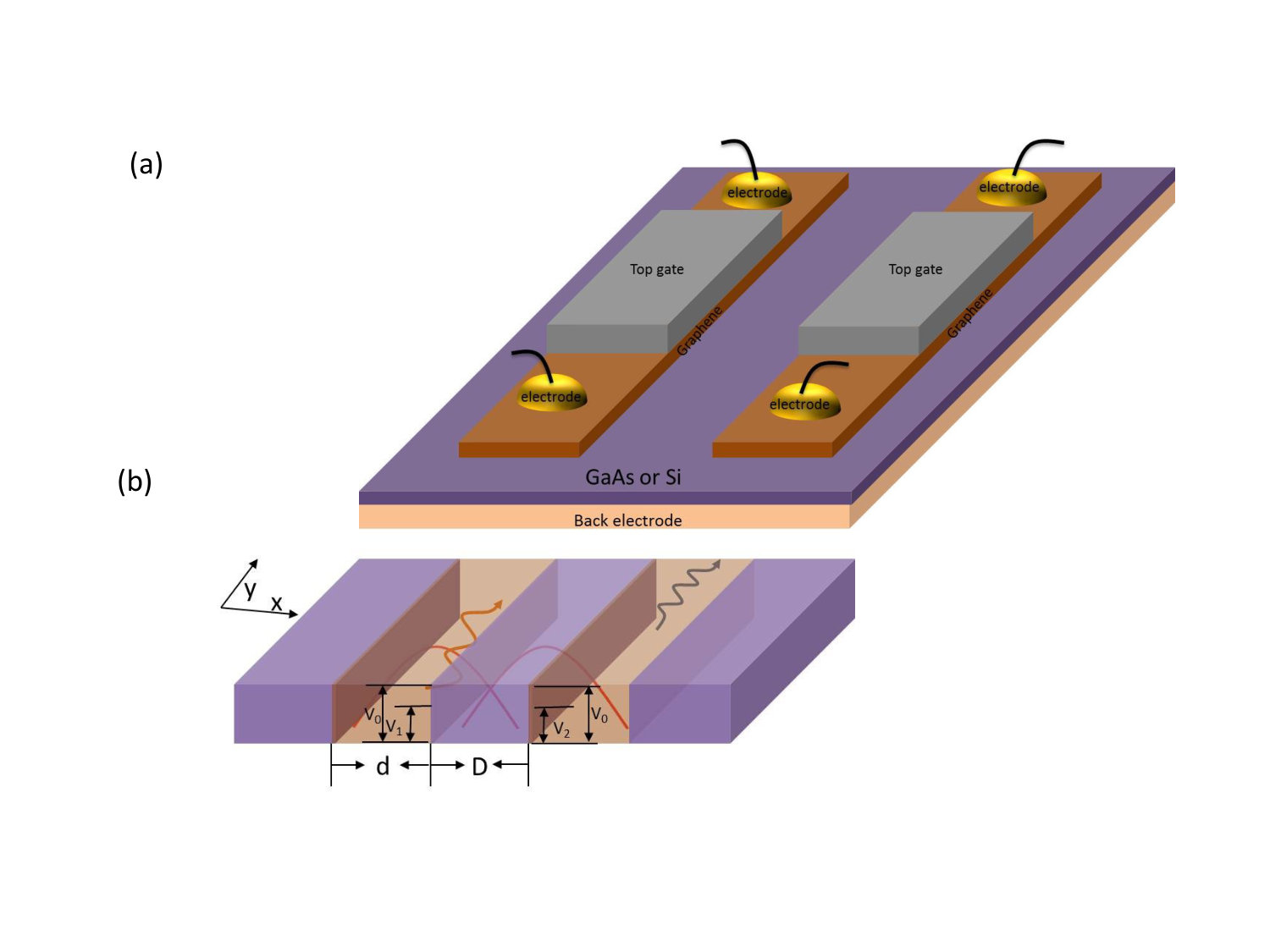 Figure 1
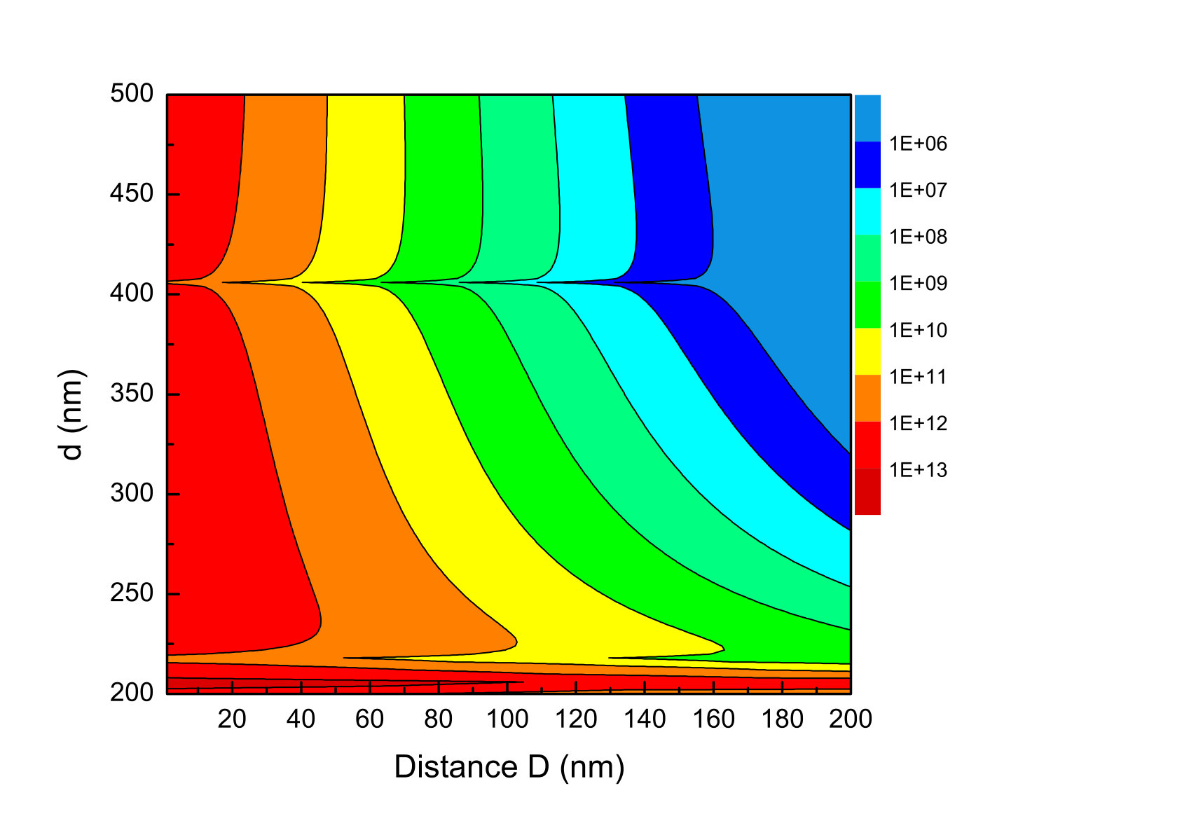 Figure 2
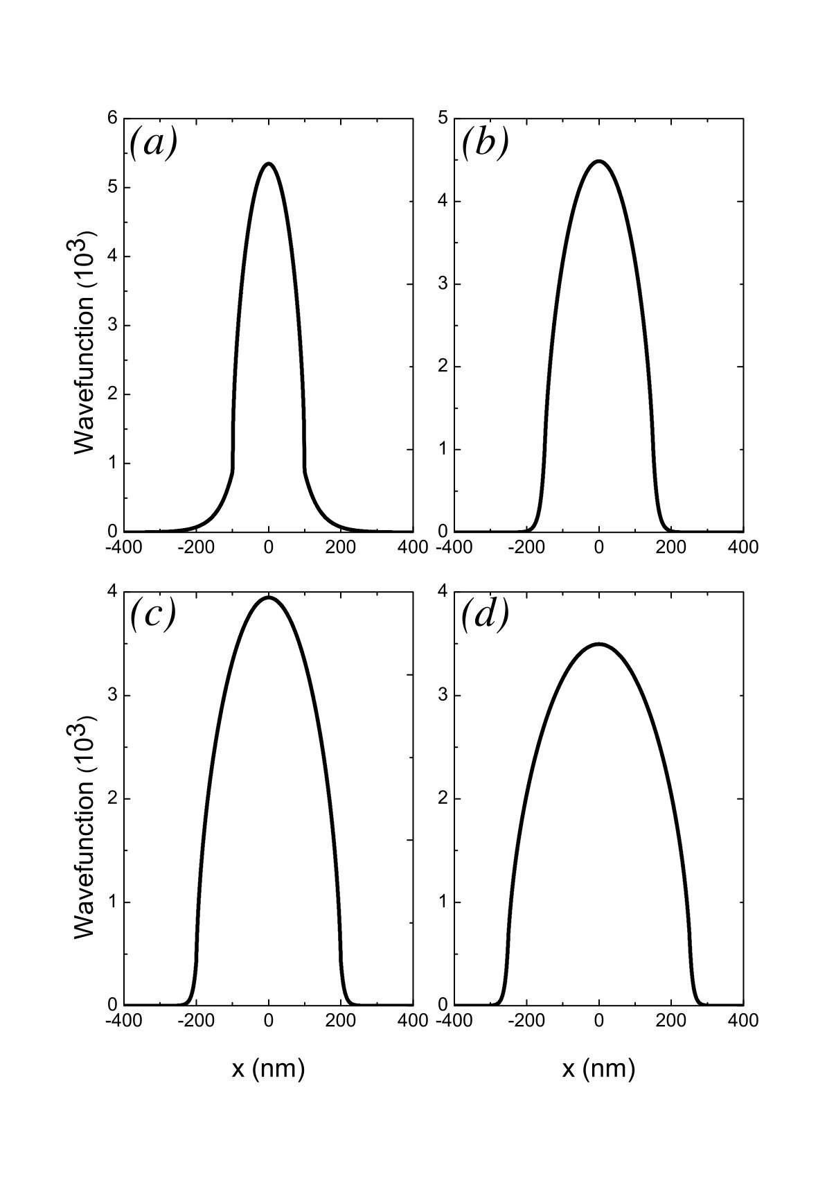 Figure 3
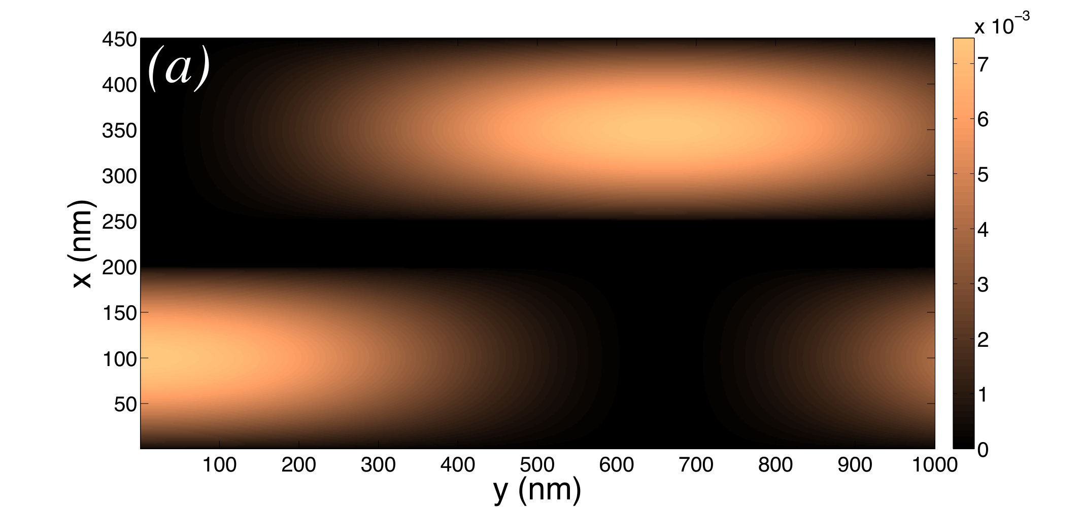 Figure 4
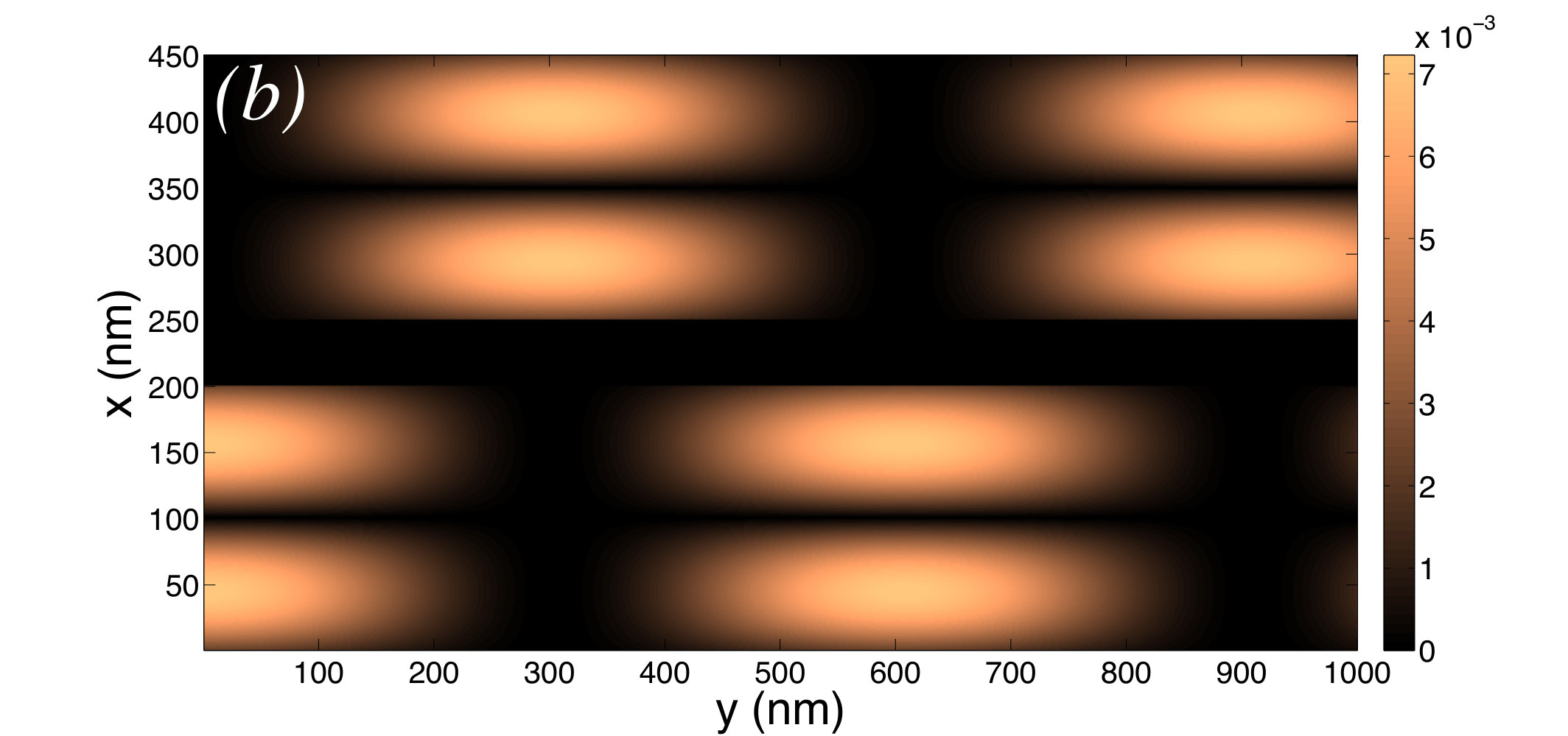 Figure 4
Peer Reviews
No public reviews on file for this paper yet. If you reviewed it on a platform where reviews are public (OpenReview, ICLR, NeurIPS, ICML), you can paste yours below so the community can read it here.
Videos
No videos yet. Explain this paper in a talk, walkthrough, or lecture? Add one.
A New Coupling Mechanism Between Two Graphene Electron Waveguides for Ultrafast Switching
Wei Huang
SUTD-MIT International Design Centre, Singapore University of Technology and Design, 8 Somapah Road, 487372 Singapore
Shi-Jun Liang
SUTD-MIT International Design Centre, Singapore University of Technology and Design, 8 Somapah Road, 487372 Singapore
Elica Kyoseva
Institute of Solid State Physics, Bulgarian Academy of Sciences, 72 Tsarigradsko Chaussée, 1784 Sofia, Bulgaria
Lay Kee Ang
SUTD-MIT International Design Centre, Singapore University of Technology and Design, 8 Somapah Road, 487372 Singapore
Abstract
In this paper, we report a novel coupling between two graphene electron waveguides, in analogy the optical waveguides. The design is based on the coherent quantum mechanical tunneling of Rabi oscillation between the two graphene electron waveguides. Based on this coupling mechanism, we propose that it can be used as an ultrafast electronic switching device. Based on a modified coupled mode theory (CMT), we construct a theoretical model to analyze the device characteristics, and predict that the switching speed is faster than 1 ps and the on-off ratio exceeds . Due to the long mean free path of electrons in graphene at room temperature, the proposed design avoids the limitation of low temperature operation required in the traditional design using semiconductor quantum-well structure. The layout of our design is similar to that of a standard CMOS transistor that should be readily fabricated with current state-of-art nanotechnology.
I Introduction
Graphene’s extremely-high mobility enables the promising application in electronics, but it is notoriously difficult to have a high turn on and off ratio due to the lack of a band gap for single-layer field-effect transistors (FET) Meric08 ; Avouris10 . There have been some extensive research activities in the exploration of novel approaches to achieving high on-off ratios graphene FET, such as utilization of uniaxial strain Ni08 , lateral confinement Zhou07 and breaking inversion symmetry Zhang09 , in order to create a band gap in single-layer graphene. Another approach is to exploit transport band gap based on few-layer graphene under perpendicular electric field Xia10 . A recent approach utilizes the unique electron transport in graphene, called electron optics mechanism in p-n Junctions Chen16 ; Sajjad11 . Unfortunately, the on-off ratio of graphene FET based on above proposals is still lower than even at higher large bias Britnell2012 ; Ghobadi2014 .
In this paper, we will explore the coupling between two graphene electronic waveguides based on the coherent quantum mechanical tunneling of Rabi oscillation The concept of electron waveguide was first proposed in the 90s in analogy to the optical waveguide Alamo1990 ; Tsukada1990 ; Kroemer1989 ; Alamo1998 ; Eugster1991 ; Liang2001 ; Hrebikova2014 , where the electrons are trapped in a quantum well structure composed of AlGaAs/GaAs material and ballistic electron transport is assumed. Based on this electron waveguide with AlGaAs/GaAs quantum well structure, the researchers described the coupling mechanism between two electron waveguides based on coupled mode theory (CMT) and proposed the concept of electron switching device based on electron waveguide. These types of electron waveguide switches are expected to have ultrafast operating speed. Recent calculations show that the operating frequency of such a device is up to s*-1* and the maximum coupling energy between the waveguides is 10 meV Tsukada1990 ; Kroemer1989 , which corresponds to a very short coupling length of about 280 nm. Despite these encouraging predictions, it has never been realized experimentally at room temperature probably due to the unjustified assumption of long electron mean free path at the interface of AlGaAs/GaAs material at room temperature that the electrons will suffer inelastic scattering and the coherent phase of the wave packet can not be maintained. Thus, an electron waveguide based on AlGaAs/GaAs materials at room temperature may not be practical for ultrafast switching application as ultra-low temperature (typically below 4K) is required Alamo1998 .
This limitation may be lifted with the advances in using graphene electron waveguide Zhang2009 ; Hartmann2010 ; Rickhaus2013 ; Williams2011 ; Allen2016 , which have successfully demonstrated ballistic electron transport in a quantum well created on graphene on the length scale of a few m. Tunable Fermi level in the graphene via gating voltage will also offer additional control over the performance of electronic switching device as the tunable barrier height formed at the interface of graphene and different semiconductors (e.g. Si and GaAs) has been confirmed both experimentally and theoretically SBH ; SBH1 ; Liang2015 ; Ang2016 , and thus provides another advantage over the fixed band offset at the interface of AlGaAs/GaAs material. All these new findings may enable a high on-off ratio electronic switching device by using graphene-based electron waveguide.
In this paper, firstly, we introduce coupled mode theory (CMT) to determine the coupling between two parallel graphene electron waveguides, which may serve as a novel ultrafast electronic switching device, in analogy to the optical dual-channel waveguide device. The schematic diagram of the proposed design is shown in Fig.1. As compared to the AlGaAs/GaAs quantum well structure, there are three main advantages as summarized below. Firstly, graphene electron waveguide has long electron mean free path, about 4 to 10 m MFPT1 at room temperature, which may be larger than the characteristic length of the device. Secondly, graphene material has tunable Fermi energy level via gating voltage. Lastly graphene electron waveguide can operate at room temperature. According to our calculated results (see Figs. 2 and 3), we predict that the switching time is faster than 1 ps (as shown in Fig.4) and a very high on-off ratio (exceeds , as shown in Fig.5).
II Coupled mode theory of graphene electron waveguide
Coupled-mode theory (CMT) was initially developed for guided-wave optics to describe the coupling between adjacent optical waveguides, due to the overlap of their evanescent electromagnetic fields. This allows light to be transferred robustly between the optical waveguides Yariv1973 ; Longhi2005 ; Huang2014 . By drawing the analogy between the wave nature of electrons (as massless particles) traveling inside the graphene to electromagnetic waves in optical waveguides, CMT is revised to describe the coupling between two parallel graphene electron waveguides as shown in Fig.1. When the graphene electron waveguides are closely positioned, electrons can be efficiently coupled. For the proposed electron switching device, we assume that the two bias gate voltages and are equal, thus realizing an electron tunneling version of the Rabi oscillations. Based on CMT, the coupling length will depend on a coupling parameter defined as (see definition below) between the two graphene waveguides, namely , where is integer, is the transition frequency, and m/s is the Fermi velocity of electrons in graphene.
In our two-dimensional (2D) model (see Fig. 1), the proposed ultrafast quantum field-effect transistor (FET) behaves like an electron switching device consisting of two parallel graphene electron waveguides. The width of the waveguide is and the separation of the two waveguides is . Aligned with the standard complementary metal-oxide-semiconductor (CMOS) FET terminology, the two parallel graphene waveguides can be regarded as a source waveguide and a drain waveguide. For each graphene waveguide, the two ends are referred as its input and output for the electrical signal. The ohmic contact between the metal electrodes and the graphene is assumed to enable sufficient electron injection into the waveguides.
When a small voltage is applied to the left graphene waveguide, an electrical current can be measured at the outputs of both graphene waveguides. The gate voltages ( and ) on each graphene waveguide are used to tune the Fermi level of each channel independently. Consequently, the Schottky barrier height () and thickness layer () between the graphenes can be modulated. If the Schottky barrier height and the effective gap spacing between the two graphene waveguides are sufficiently small, the evanescent wave of the injected electrons in the source waveguide can tunnel into the drain waveguide with some probability as represented by the red curve in Fig. 1b, which can be defined as an on-state. When the Schottky barrier height and effective gap spacing become large due to the applied gate voltage, the tunneling probability of electron tunneling from source waveguide to drain waveguide is extremely small, which can be defined as an off-state (In our example, we set off-state of gate voltages as 300 meV). Note that the phase of the electrons is maintained during the tunneling process. Quantum mechanically, the injected electrons in the source waveguide can be detected at the drain waveguide with a probability equal to 1 [see black curved arrow in Fig. 1 (b)] at a certain transfer length .
In our model, we assume that a quantum well is created at the interface between the graphene and GaAs. The electrons in the graphene waveguides are confined along with the -direction, and they unbounded in the -direction. The total electron wave function is the superposition of all possible quantum eigenstates. We make the notations () as the electron wave function of source (drain) graphene waveguide, which is written as
[TABLE]
where , are , modes with respect to source/drain graphene waveguide. Here, , are the mode profiles of the wavefunctions determined by electron eigenstates in the quantum well, where are the mode indexes. and are the respective propagation constants of the and modes in graphene electron waveguide with respect to source/drain graphene waveguide. The parameters and describe the injection electron angles with respect to the corresponding and modes in the source/drain graphene waveguide, and are the wave vectors of electron injected in the source/drain graphene waveguide: and . The wave vector in the barrier material is , where is the electron energy and is the electron effective mass in the semiconductor material.
According to Myoung’s paper Myoung2011 , the electron’s wave function behaves as a plane wave along with the direction and Eq. (1) can be rewritten as
[TABLE]
where = and =. In the direction, the motion of the electrons in the graphene electron waveguides is described by the 1D free electron Dirac equation, which allows us to decouple the wavefunctions into two sublattices: A and B wave functions (see the Appendix for details). Finally, two Helmholtz-like equations in the direction are obtained as
[TABLE]
Based on the CMT model Yariv1973 we can manipulate the Helmholtz equations to obtain
[TABLE]
which are consistent with previous optical waveguide coupled equations Saleh1991 and the electron waveguide coupled equations Alamo1990 .
By substituting Eq.(1) into the Eq.(4), and considering and obeying Eq.(3), we apply the slowly envelope varying approximation Saleh1991 to Eq. (4), such that and , and obtain the following coupling equations:
[TABLE]
Here, and are the coupling coefficients, which are given by,
[TABLE]
Finally, Eq.(5) can be rewritten as a Schrödinger-like equation of a two-level system,
[TABLE]
where . It is important to note that Eqs. (6) and (7) are the master coupling equation for determining the coupling between mode and mode in source/drain graphene electron waveguide studied in this paper. They are valid for the coupling of any dual-graphene electron waveguide device.
Before presenting the results, it is important to note that graphene is used as the electron waveguide channel and GaAs is the material for the potential barrier. The electrons inside the graphene waveguide channels are described by Dirac equation and Schrödinger equation is used to describe electrons dynamics in the potential barrier (GaAs). Previous work on single graphene electron waveguide channel Zhang2009 ; Hartmann2010 ; Yuan2011 ; Myoung2011 has shown that the evanescent electron wave will exponentially decay outside of graphene electron waveguide. According to Hartmann’s Hartmann2010 and Xu’s Xu2015 papers, there are two kinds of stable modes in graphene electron waveguide dependent on two sub-lattice modes: and , where is anti-symmetric and is symmetric. The coupling between the same anti-symmetric functions, and the coupling between the antisymmetric and symmetric functions is, respectively, 0.24 meV and 0.14 meV, which are much smaller than the coupling between the two symmetric functions (1.58 meV).
Thus, we only consider the coupling of two symmetric functions in this paper. In Fig. 2, we show the symmetric wave function of the graphene electron waveguide at the different width of the waveguide: = 200, 300, 400, and 500 nm. The probability current density through the interface of graphene and GaAs is conserved Dragoman2013 . Unless specified, the default parameters are =500 meV, =450 meV, and = 4.96 is defined as the wave vector in the direction.
The coupling strength between two parallel graphene electron waveguides is shown in Fig. 3, where we have assigned and study the dependence as a function of spacing () between the waveguides and width of the waveguide . From Fig. 3, the coupling strength is decreasing with increasing spacing of from about 0 to 120 nm. The coupling also increases with decreasing from 500 nm to 250 nm. For smaller = 250 nm or smaller, the mode profile becomes flat, and the overlapping calculated by initially decreases until reaching a critical point, which is determined by the energy and incident angle as well as barrier height of injected electron. Finally we show a contour plot of the transition frequency as a function of the spacing and in Fig. 4.
Compared with prior electron switching devices based on AlGaAs/GaAs materials, our proposed design based on graphene waveguides will have larger coupling energy (around 15 meV) and faster operating frequency ( 1 ps in terms of time scale) as shown in Fig. 4. Most importantly, our proposed device is able to operate at room temperature due to the long mean free path of electrons in the graphene as compared to AlGaAs/GaAs material.
III Discussions
Previous graphene field effect transistors have the low on-off ratio at room temperature Schwierz2010 . In spite of many efforts to improve their designs Britnell2012 ; Ghobadi2014 ; Wang2015 ; Katkov2014 , the on-off ratio of the graphene field effect transistors is still below even at a relatively high voltage of the order of 5 V Britnell2012 ; Ghobadi2014 . From the results obtained above in this paper, our proposed design can behave as a field effect transistor, in which electrons coupling between the two waveguides can be controlled by the gate voltage. Typical values of the on-off ratio is presented in Fig. 5, in which we use = 50 nm and =200 nm and . From the figure, we see that the on-off ratio can exceed .
From solving Eqs. (6) and (7) numerically, we present the first and second coupling modes of the graphene waveguide in Fig. 6 for = 200 nm and = 50 nm For simplicity, the detuning parameter is set at and thus . The Schottky barrier height between the graphene and the GaAs is 0.5 eV SBH1 . In general, higher barrier height will allow for a lower coupling strength , and leads to a longer coupling length. We also assume that the symmetrical wave mode is the initially populated mode in the source graphene waveguide, which can be coherently excited by the high-quality contact between the metal electrode and graphene.
Figure 6 clearly shows a demonstration of Rabi oscillations of the electrons probability amplitudes between the two graphene waveguides, in analogy to the dynamics of a two-level quantum mechanical system. The population of the different modes of the graphene waveguides depends on the gate-controlled guiding of the electrons into the source waveguide. If the electron injected into the source graphene waveguide has a wave packet perfectly matched at a certain waveguide eigenstate, only that specific mode will be excited. The figure also demonstrates the electron coupling transfer length up to 1000 nm is possible. As an example, the coupling between the first modes in quantum optical waveguides, the coupling length is nm with a transfer frequency of s*-1* (or 0.65 ps), which is very fast (less than 1 ps).
These results show that the proposed electron switching device based on graphene electron waveguides has considerable advantages compared to similar devices using the conventional semiconductors materials in terms of operating speed, compactness and operating at room temperature. Note we do not consider higher-order coupling between the first mode in source waveguide and the second mode in the drain waveguide. The reasons are two folds: firstly, the coupling between the first mode (in the source waveguide) and second modes (in the drain waveguide) is asymmetric leading to very weak coupling strength (0.12 meV). Secondly, the preparation of modes in the waveguides (source or drain) depends on specified electron injection angles, so it is difficult to implement experimentally the coupling between these two modes. Interestingly, the coupling transfer length will be reduced to = 302 nm and the transfer frequency will increase to s*-1* (0.3 ps) for coupling only between the second modes in the graphene electron waveguide, as shown in the Fig.6 (b).
CMT is a very powerful method to compute coupling strength, for which the only assumption is that two mode profiles would not have changed during overlapping of two evanescent electric fields of two optical waveguides Yariv1973 ; Haus91 . The CMT not only works well for the electric field, also for electron wave function described by quantum mechanics. For example, the coupling mechanism of superconducting Josephson junctions can be described by CMT, as the evanescent wave function of electrons in two superconductors has overlapping Raghavan99 ; Similarly, the CMT has also been utilized to describe the coupling between electronic waveguides based on AlGaAs/GaAs materials. Furthermore, the previous work on graphene electronic waveguide has already shown that wave function of electrons has the similar mode as the optical waveguide Hrebikova2014 ; Zhang2009 ; Hartmann2010 ; Rickhaus2013 ; Williams2011 , [see electron wave function modes in graphene (Fig. 2)]. Based on these arguments above, we believe that the CMT is valid for the description of the coupling mechanism between two parallel graphene electron waveguides.
There have been various papers Gorbachev2012 ; Schutt2013 ; Tse07 ; Kim2011 pointing out that Coulomb drag effect is very profound near the Dirac cone, which is induced by strong electron-electron interaction between two horizontal parallel graphene sheets separated by dielectric materials. However the graphene layout in our proposed device is coplanar parallel instead of horizontal parallel. Besides we focus on the condition that the Fermi level is far from the Dirac point. From the following simple analysis of Coulomb drag effect, we find that the Coulomb drag effect plays a minor role in our model.
When a current flows on the active layer of graphene, it will induce a voltage on the passive layer of graphene, due to Coulomb drag effect, which can be measured by drag resistivity . To numerically estimate the effect of the drag effect in our system, the drag resistivity based on Boltzmann transport formalism and the random phase approximation is used Tse07 ; Kim2011 , which is
[TABLE]
Here, subscripts 1 and 2 are the labels for the two single-layer graphenes and is the nonlinear susceptibility of layer . is the screened interlayer potential in the random phase approximation. is the longitudinal conductivity of the layer and is the Boltzmann constant. The current flow in the passive graphene layer caused by coulomb drag can be estimated as, , where denotes the conductivity of the passive graphene layers adam2007 , is the width of our graphene layer and is the scattering time. For a typical set of parameters: nm, K, nm and meV, we get the ratio of is 0.18 %, which is extremely small. Thus the Coulomb drag effect in our model is negligible and will not greatly affect the calculations reported in this paper.
Due to the electrons scattering, the phase of electrons will be randomly changed. However, we can estimate the phase coherence length of electron in semiconductor at room temperature. If our device setting up of distance between two graphene (D = 50 ) is smaller than the phase coherence length of electron, we can ignore the phase changing of the electrons. The phase coherence length of electron can be described by the equation, Altshuler1982 ; Aleiner1999 , where is the diffusion coefficient and is the boltzmann constant. At the ultra-low temperature, the phase coherence length can be up to 18 Topinka2001 . By substituting room temperature (T = 300 ) and geometry setting up of our device (L = 654 ) into the equation, we can obtain the phase coherence length is around 80 , where the diffusion coefficient is given by Einstein relation . Therefore, our estimated phase coherence length =80 is larger than distance between two graphene (D = 50 ) and we can ignore the phase changing of the electron in our configuration. Furthermore, this result is corresponding to electron-phonon collisions rate is around , where our switch time is 1 and this electron-phonon collisions rate is consisting with experiment date Muhammad2017 .
Conventional graphene electrical switches are mainly based on the field effect transistor Meric08 ; Avouris10 ; Ni08 ; Zhou07 , which utilizes the tunneling effect in the conduction channel between the source and drain electrodes. Unlike those conventional switches, the proposed electrical switch is not based on this traditional principle although its configuration is similar to conventional field effect transistors. The operating principle of our electrical switch depends on the electron wave coupling between the source graphene electron waveguide and the drain waveguide, which exhibits Rabi oscillations.
To check the sensitivity of the device against the fluctuations in the chemical potential, we assumed that the variation of the chemical potential is about meV. Our calculations show that the resulting variation in the on-off ratio is less than . Large chemical potential can ensure the stable operation of the proposed electrical switch without being affected by external environmental factors. The variation of meV in the Fermi level may be justified by the large Fermi level. Previous paper Hajaj2013 has reported that fluctuations in the carrier density induced by impurities in the environment or other factors disappear and chemical potential distribution becomes homogeneous when Fermi level is far from the neutral point in the graphene. If it is near the Dirac cone of the graphene, while fluctuations in the chemical potential may affect the operation of our device.
Additionally, the distance between two electron waveguide sets to be larger than 50 nm, so that the coupling between the two graphene sheets is too weak to open a gap in the graphene electronic bandstructure. Both theory and experiments have an already confirmed that a very weak coupling between two separated graphene sheets cannot lead to a band gap if the gap distance between two graphene sheets is beyond 10 nm Magda2014 ; Zhao2011 . Importantly, it is worth to emphasize that the proposed device operates at room temperature adam2007 ; qiuzhi2011 , as a result, the exchange interaction between the electrons will be smeared out by large temperature fluctuations.
IV Conclusion
In summary, we have studied the coupling between two graphene electron waveguides by utilizing coupled mode theory (CMT). Based on this coupling mechanism, we have proposed an ultrafast electron switching device based on a dual-graphene-electron-waveguides structure. The performance of this design is analyzed by using a modified couple model theory together with solving the Dirac and Schrödigner equations. Based on our model, it is possible to achieve higher operating frequency (less than 1 ps time scale) with short coupling transfer length at room temperature. This performance is better than the conventional design in using traditional AlGaAs/GaAs quantum well structure, which will also require very low operating temperature in order to have a long electron mean free path to ensure ballistic electron transport. The proposed design can be realized using current state-of-art-technology, for example single graphene electron waveguide channels have recently been fabricated with the gate-controlled guiding of electrons Williams2011 . Our design resembles the traditional CMOS transistor in its layout, and thus its fabrication is feasible and it has the potential to contribute to the rapid development of quantum circuits and other integrated electron devices.
V Acknowledgment
This work is partially supported by the Singapore ASTAR AME IRG (A1783c0011) and USA Air Force Office of Scientific Research (AFOSR) through the Asian Office of Aerospace Research and Development (AOARD) under Grant No. FA2386-17-1-4020. EK acknowledges financial support from the European Union’s Horizon 2020 research and innovation programme under the Marie Skłodowska-Curie grant agreement No 705256 — COPQE.
VI Appendix
Firstly, we show that the Helmholtz-like equations (Eq. (3)) can be described as source/drain graphene electron waveguide in the direction propagation. We take the source graphene electron waveguide as an example in our derivation and only consider single mode. Two sublattices A and B’s wavefunction of source graphene electron waveguide refer to as and . Electron is unbounded in the -direction and electron’s energy is , where is electron injection angle of source graphene electron waveguide. Based on the Dirac equations for free particles, we have
[TABLE]
Equation (A1) can be rewritten as and , with . By taking the derivative on both side of the equations to decouple and , we obtain the Helmholtz-like equation for the source graphene electron waveguide: and .
For source graphene electron waveguide, we only consider , and the governing equation becomes . Repeat the same procedure, the Helmholtz-like equation for the drain graphene electron waveguide is obtained as .
Below we show the derivation of Eq. (5) from Eq. (4) in the main text.
[TABLE]
In Eq. (A2), we apply slowly envelope varying approximation Saleh1991 , say and . Slowly envelope varying approximation (SEVA) is valid, when assume that the envelope of a forward-travelling wave pulse varies slowly in time and space compared to a period or wavelength. We can estimate the smallest envelope size in our configuration, around 13 nm Shafraniuk2015 , which are much larger than wavelength of electron in graphene, 0.74 nm Meyer2008 . Therefore, slowly envelope varying approximation is a good approximation in our paper. Slowly envelope varying approximation is very widely used method in the optics wave Yariv1973 ; Longhi2005 ; Huang2014 and the slowly envelope varying approximation also can work for the electron wave function Burt1999 . We can ignore the first term. The third term and fourth terms can be cancelled out each other, based on Eq. (A2).
The reference list from the paper itself. Each links out to its DOI / PubMed record.
- 1(1) I. Meric, M.Y. Han, A.F. Young, B. Ozyilmaz, P. Kim and K.L. Shepard, Nature nanotechnology , 2008, 3 , 654-659.
- 2(2) P. Avouris, Nano letters , 2010, 10 , 4285-4294.
- 3(3) Z. Ni, T. Yu, Y. Lu, Y. Wang, Y. Feng and Z. Shen, ACS nano , 2008, 2 , 2301-2305.
- 4(4) S.Y. Zhou, G. Gweon, A.V. Fedorov, P.N. First, W.A. de Heer, D.H. Lee, F. Guinea, A.H. Castro Neto and A. Lanzara, Nature Materials , 2007, 6 , 770 - 775.
- 5(5) Y. Zhang, T. Tang, C. Girit, Z. Hao, M. Martin, A. Zettl, et al. Nature , 2009, 459 , 820-823.
- 6(6) F. Xia, D. Farmer, Y. Lin and P. Avouris, Nano letters , 2010, 10 , 715-718.
- 7(7) S. Chen, Z. Han, M.M. Elahi, K. M. Habib, L. Wang, et al, Science , 2016, 353 , 1522-1525.
- 8(8) R. Sajjad and W. Avik. Applied Physics Letters , 2011, 99 , 123101.