Noise-enhanced chaos in a weakly coupled GaAs/(Al,Ga)As superlattice
Zhizhen Yin, Helun Song, Yaohui Zhang, Miguel Ruiz-Garcia, Manuel, Carretero, Luis L. Bonilla, Klaus Biermann, and Holger T. Grahn
TL;DR
This paper demonstrates that external noise can induce and enhance chaotic current oscillations in a GaAs/AlGaAs superlattice at room temperature, supported by experiments and simulations based on a nonlinear tunneling model.
Contribution
It provides the first detailed experimental and simulation evidence of noise-induced chaos in a weakly coupled superlattice at room temperature.
Findings
Noise increases the range of bias voltages with chaotic oscillations.
Chaotic spikes are triggered by small fluctuations at domain boundaries.
Simulations qualitatively match experimental observations.
Abstract
Noise-enhanced chaos in a doped, weakly coupled GaAs/Al_{0.45}Ga_{0.55}As superlattice has been observed at room temperature in experiments as well as in the results of the simulation of nonlinear transport based on a discrete tunneling model. When external noise is added, both the measured and simulated current-versus-time traces contain irregularly spaced spikes for particular applied voltages, which separate a regime of periodic current oscillations from a region of no current oscillations at all. In the voltage region without current oscillations, the electric field profile consist of a low-field domain near the emitter contact separated by a domain wall consisting of a charge accumulation layer from a high-field regime closer to the collector contact. With increasing noise amplitude, spontaneous chaotic current oscillations appear over a wider bias voltage range. For these bias…
Click any figure to enlarge with its caption.
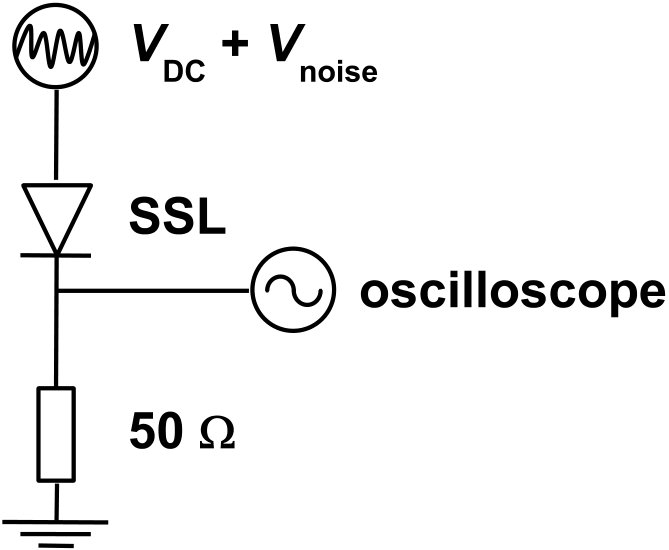 Figure 1
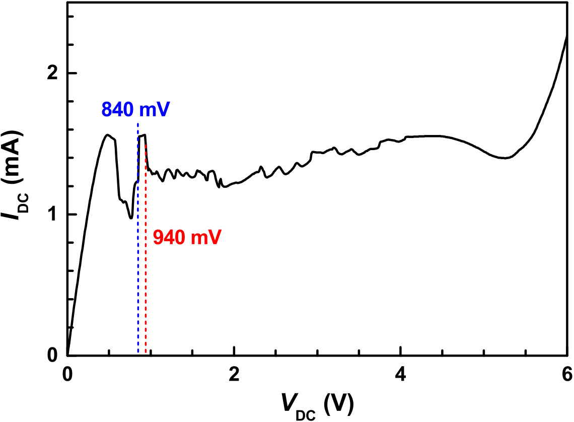 Figure 2
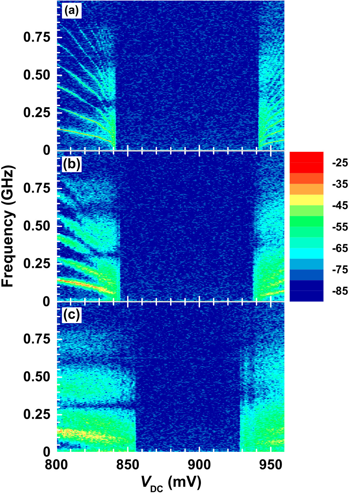 Figure 3
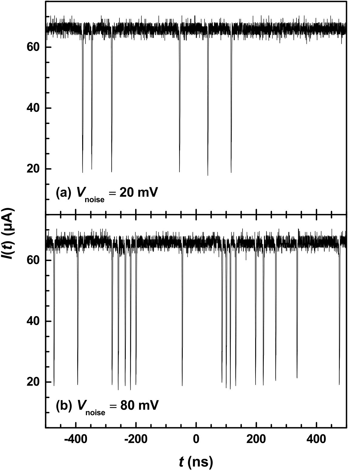 Figure 4
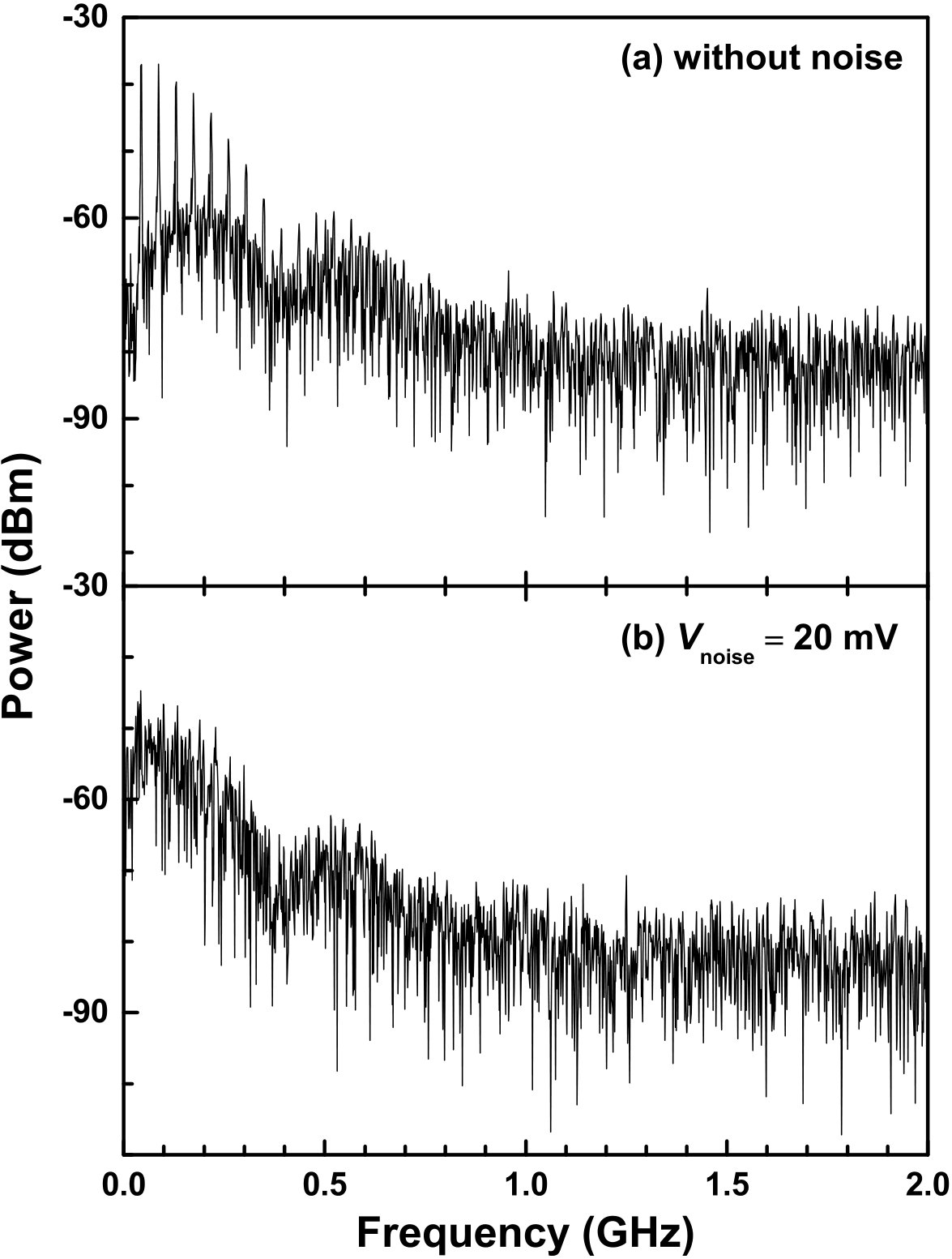 Figure 5
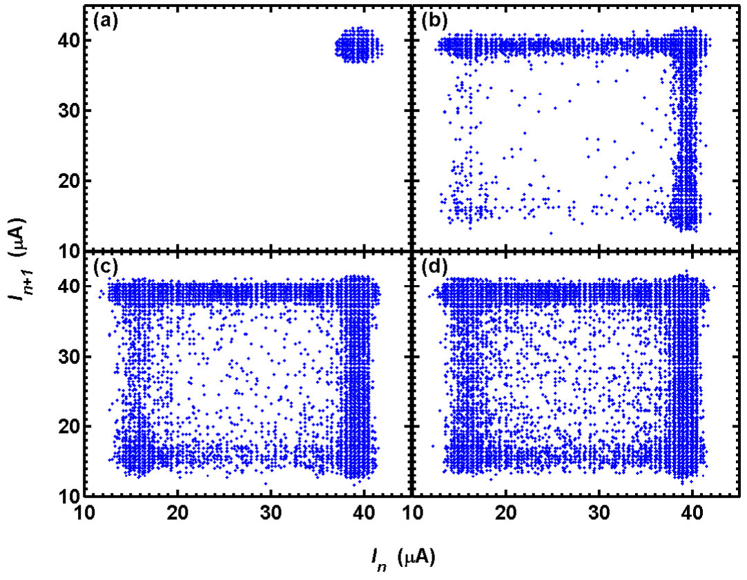 Figure 6
 Figure 6
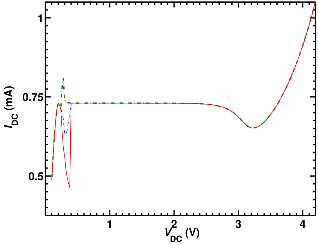 Figure 7
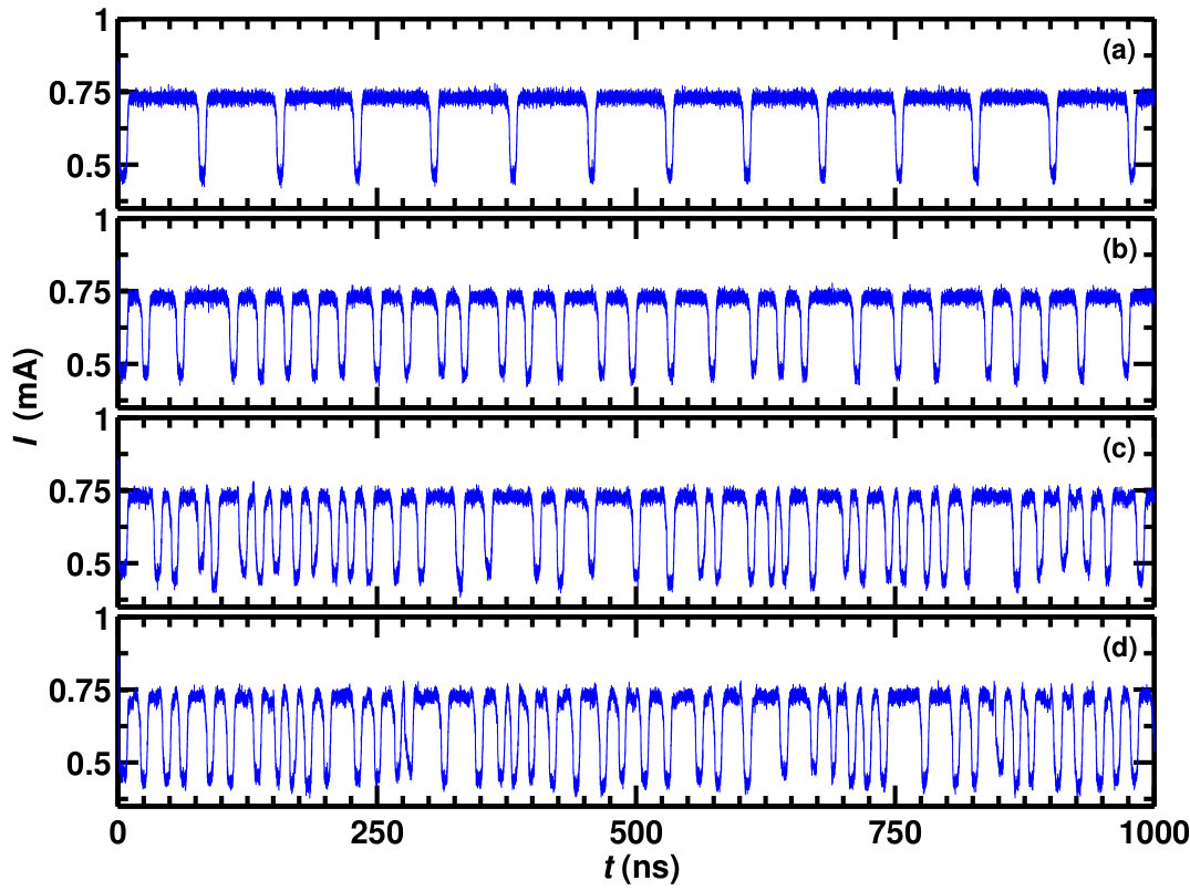 Figure 8
 Figure 8
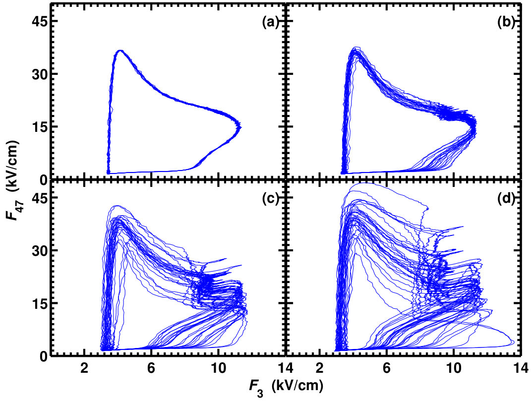 Figure 9
| (meV) | (meV) | (meV) | (meV) |
|---|---|---|---|
Peer Reviews
No public reviews on file for this paper yet. If you reviewed it on a platform where reviews are public (OpenReview, ICLR, NeurIPS, ICML), you can paste yours below so the community can read it here.
Videos
No videos yet. Explain this paper in a talk, walkthrough, or lecture? Add one.
Noise-enhanced chaos in a weakly coupled GaAs/(Al,Ga)As superlattice
Zhizhen Yin
Helun Song
Yaohui Zhang
Key Laboratory of Nano devices and Applications, Suzhou Institute of Nano-tech and Nano-bionics, Chinese Academy of Sciences, Suzhou 215125, China
Miguel Ruiz-García
Manuel Carretero
Luis L. Bonilla
Gregorio Millán Institute, Fluid Dynamics, Nanoscience and Industrial Mathematics, Universidad Carlos III de Madrid, 28911 Leganés, Spain
Klaus Biermann
Holger T. Grahn
Paul-Drude-Institut für Festkörperelektronik, Leibniz-Institut im Forschungsverbund Berlin e. V., Hausvogteiplatz 5–7, 10117 Berlin, Germany
Abstract
Noise-enhanced chaos in a doped, weakly coupled GaAs/Al0.45Ga0.55As superlattice has been observed at room temperature in experiments as well as in the results of the simulation of nonlinear transport based on a discrete tunneling model. When external noise is added, both the measured and simulated current-versus-time traces contain irregularly spaced spikes for particular applied voltages, which separate a regime of periodic current oscillations from a region of no current oscillations at all. In the voltage region without current oscillations, the electric field profile consist of a low-field domain near the emitter contact separated by a domain wall consisting of a charge accumulation layer from a high-field regime closer to the collector contact. With increasing noise amplitude, spontaneous chaotic current oscillations appear over a wider bias voltage range. For these bias voltages, the domain boundary between the two electric-field domains becomes unstable, and very small current or voltage fluctuations can trigger the domain boundary to move toward the collector and induce chaotic current spikes. The experimentally observed features are qualitatively very well reproduced by the simulations. Increased noise can consequently enhance chaotic current oscillations in semiconductor superlattices.
I Introduction
With the continuous advancement of nonlinear science and the theory of random dynamical system, we have become aware of the fact that noise should not always be considered as a disturbing factor. Actually, a small amount of noise may enhance the dynamics of a system so that it becomes better defined and controllable. Constructive effects of noise in nonlinear systems have been investigated extensively in the context of stochastic resonances and coherence resonances. By stochastic resonance, noise can optimize the response of a system to an external signal and induce stochastic phase synchronization to the external force wie95 ; gam98 . For a coherence resonance, pure noise without an external signal can generate the most coherent motion in the system, as has been mainly observed in excitable systems hu93 ; zho01 .
A doped, weakly coupled semiconductor superlattice (SSL) represents an almost ideal spatially one-dimensional nonlinear dynamical system with a large number of degrees of freedom, the nonlinearity of which is due to sequential resonant tunneling between adjacent quantum wells. Fluctuations of the layer thicknesses, electron density, energy levels, and inter-well coupling transform a weakly coupled SSL into a complex nonlinear system, in which the electron transport is strongly dissipative. A great richness of nonlinear transport behavior has been observed in weakly coupled SSLs, including the formation of stationary electric-field domains, periodic as well as quasi-period current self-oscillations, and even driven as well as undriven chaos bon02 ; bon05 . The oscillatory behavior is attributed to the localized, oscillatory motion of the domain boundary, which separates the high from the low electric-field domain. Only very recently, spontaneous chaotic hua12 and quasi-periodic hua13 current self-oscillations were observed at room temperature in GaAs/(Al,Ga)As SLs using an Al content of %, which results in the largest direct barrier for this materials system.
Both theoretical and experimental results have proven that noise can affect the charge transport in weakly coupled GaAs/AlAs SLs hiz06 ; bom12 . A noise-enhanced coherence resonance has been observed in a weakly coupled GaAs/AlAs SL at K hua14 . The main reason for the existence of such a coherence resonance in such a SL is related to the interaction between the noise and the two oscillation modes existing in weakly coupled SSL oscillators such as the well-to-well hopping mode and the dipole-motion mode. On this basis, numerical simulations have shown that noise enhances spontaneous chaos at room temperature alv14 ; bon16 .
In this paper, we report clear evidence for noise-enhanced spontaneous chaos in a doped, weakly coupled GaAs/Al0.45Ga0.55As SL at room temperature. We find that, with increasing noise amplitude, the spontaneous chaotic oscillations appear over a wider range of voltages. The experimentally observed results are qualitatively very well validated by numerical simulations based on a discrete resonant tunneling model that captures the main features of vertical transport in doped, weakly coupled SSLs alv14 ; bon16 . The paper is organized as follows. In the next section, we describe the sample structure and measurement techniques followed by the experimental results of the current-voltage characteristics, the current self-oscillations, and attractors extracted from the experimental results. In Sec. III, we present the discrete resonant-tunneling model and the results of the numerical simulations. Finally, we summarize the obtained results and conclude in Sec. IV.
II Experimental results
II.1 Sample structure and measurement techniques
The sample consists of a doped, weakly coupled GaAs/(Al,Ga)As SL with periods, each period consisting of a GaAs quantum well and an Al0.45Ga0.55As barrier. The central nm of each -nm-thick GaAs well are doped with Si at a density of 2$$\times$$10^{17} cm*-3*. The thickness of the Al0.45Ga0.55As barriers is nm, resulting in a rather weak coupling between adjacent quantum wells. The SSL is sandwiched between two highly doped GaAs contact layers forming an -- diode. For more details of the sample structure, see Ref. li15, . After plasma etching and providing Ohmic contacts of AuGe/Ni/Au with nm using electron beam evaporation followed by rapid thermal annealing at C, square mesas with a side length of m are investigated. Single devices are wire bonded for electrical measurements. All experimental measurements are performed at room temperature. The DC bias voltage and the noise with amplitudes are applied using the function generator Agilent 33220A. The current-time traces and the frequency spectra are recorded with a GHz oscilloscope LeCroy Wavepro 760Zi-A. For the current-time traces, the oscilloscope records voltage pulses, which are then converted in current values using the - characteristics. A schematic of the measurement circuit is shown in Fig. 1, which is the same as the one in Ref. hua14, .
II.2 Current-voltage characteristics
A typical current-voltage characteristic of the the doped, weakly coupled SSL device is shown in Fig. 2. In the voltage range between and mV, the DC current rapidly increases from to mA, followed by a current plateau between and mV. In this voltage range, electric-field domains are formed with a charge accumulation layer forming the domain boundary. As the voltage increases further to mV, the current decreases to mA and then continues down to mA.
II.3 Current self-oscillations and frequency spectra
The frequency spectra displayed in Fig. 3(a) recorded between and mV without any external noise do not show any current self-oscillations for values between and mV. For values outside this region, i. e., smaller than or larger than mV, the frequency spectra exhibit periodic oscillations with higher-order harmonics, and the fundamental frequency depends on . At and mV, where the transitions between current oscillations and no current oscillations occur, the frequency spectra are dominated by an abrupt decrease to zero frequency. These transitions are accompanied by an abrupt change of the current as shown in Fig. 2. This observation may indicate an infinite period collision of the oscillatory attractor with a homoclinic orbit. Numerical simulations confirm this scenario for the SSL model.
Figures 3(b) and 3(c) show the frequency spectra for applying additional external noise with amplitudes of and mV, respectively. For mV in Fig. 3(b), the chaotic oscillations in the transition regions appear over a larger voltage interval than without any external noise [cf. Fig. 3(a)]. The voltage region with no current oscillations becomes narrower. Increasing the noise amplitude to mV results in a further shrinkage of the voltage region with no current oscillations, and the voltage range of seemingly chaotic oscillations extends to and mV as shown in Fig. 3(c). At the same time, the frequency spectra become broader with increasing noise amplitude. These experimental data clearly demonstrate that noise can significantly enhance the chaos generated in doped, weakly coupled SSLs. This was shown theoretically for the case of internal (shot and thermal) noise by the results of the numerical simulations in Ref. alv14, . The present results show that chaos enhancement can also be achieved more generally by adding appropriate external noise.
Current traces as a function of time have been recorded for two noise amplitudes at mV as shown in Fig. 4. Note that the current traces are recorded only with AC coupling so that the information about the DC current level is lost. For mV, the current trace contains several irregularly spaced spikes as shown in Fig. 4(a). When the noise amplitude is increased to mV, the current trace exhibits more spikes with somewhat smaller amplitudes as shown in Fig. 4(b). Similar current traces are observed for mV (not shown). There are typically two oscillation modes present in doped, weakly coupled SSLs, the dipole motion mode and the well-to-well hopping mode. When the noise level is low, the dipoles are formed at the emitter moving toward the collector with a large interval of noise spikes. As the noise amplitude is increased, a continuous motion of the well-to-well hopping of the domain boundary occurs, introducing fast current oscillations in the SSL.
The power spectrum shown in Fig. 5(a) recorded at mV clearly demonstrates that, even without any external noise, the doped, weakly coupled SSL can already exhibit a broad-band spectrum, indicating the possibility of the presence of chaotic oscillations even without external noise. When noise is added as in Fig. 5(b), the power spectrum becomes even broader. At the transition regions between periodic oscillations and no oscillations, the system appears with increasing external noise amplitude to exhibit a chaotic attractor, which leads to spontaneous chaos at room temperature. As predicted by the results of the numerical simulations reported in Ref. alv14, , internal noise enhances spontaneous chaos. The same effect of chaos enhancement is observed when we add external noise with increasing amplitude as will be further discussed below. At the same time, the frequency spectra in the periodic region are dominated by an oscillation with a single frequency, but with increasing bandwidth as the noise amplitude is increased. Noise can significantly enhance the chaos generated in doped, weakly coupled SSLs.
II.4 Attractors obtained from experimental results
Figures 6(a), 6(b), 6(c), and 6(d) show reconstructed Poincaré maps from the experimental current traces versus time for no noise as well as , , and mV, respectively, at mV. In the absence of external noise, the deterministic attractor is stationary, and the Poincaré map should consist of a single point. In Fig. 6(a), the unavoidable internal noise produces many points concentrated in a small region. When external noise is added, the Poincaré maps explore a region that becomes larger and fuller as the external noise amplitude increases as shown in Figs. 6(b), 6(c), and 6(d). Similar Poincaré maps are extracted from experimental current traces versus time at mV. Figure 6(e) shows the values of the capacity dimension , the information dimension , and the correlation dimension as a function of the external noise amplitude, which all increase with increasing noise amplitude. Without external noise, the SSL is in a stationary state with zero fractal dimension. When the external noise is turned on and increased, time-dependent oscillations appear, and the fractal dimension increases abruptly demonstrating evidence of chaotic oscillations induced by noise. Figure 6(f) shows the multifractal dimension for the different noise amplitudes. For large positive values of , the fractal dimension corresponds to regions of the attractor that are more often visited by the system trajectory and does not increase that much with external noise. For and large, is due to the least sampled regions of the attractor, and it increases more strongly when the external noise increases. We conclude that increasing the external noise expands the regions in phase space that are visited by the system trajectory, an effect that is obvious from the sequence shown in Figs. 6(b)–6(d).
III Model and simulated results
III.1 Discrete resonant tunneling model
Numerical results are obtained using a discrete resonant tunneling model that captures the main features of doped, weakly coupled SSL bon02 ; bon05 . The model consists of dynamical equations describing the evolution of the variables such as the electric field as well as the two-dimensional (2D) electron density at well , the tunneling current density from well to , and the SL total current density :
[TABLE]
[TABLE]
[TABLE]
[TABLE]
[TABLE]
[TABLE]
Here , where denotes the number of periods of the SSL. The forward electron velocity is a function with peaks corresponding to the discrete energy levels in every well calculated using a Kronig-Penney model for the investigated SSL configuration as summarized in Tab. 1. A more detailed description can be found in Refs. bon05, and alv14, . The overall voltage drop between the ends of the SSL is equal to the DC voltage bias , while the noise voltage amplitude corresponds to , both provided in the experiment by the function generator in Fig. 1. The numerical values of the parameters correspond to the experimental configuration described in Sec. II with an equivalent 2D doping density due to the doping of the central part of the quantum well of N_{D}=6$$\times$$10^{10} cm*-2*. The effective mass of the electrons in the GaAs/AlxGa1-xAs SL is , where denotes the free-electron mass. The well and barrier widths are and nm, respectively, as for the experimentally investigated SSL so that the period of the SSL is nm. The transversal area of the SSL is assumed to be with m. Finally, the relative permittivity of the SSL is with and referring to the relative permittivity of the well and barrier material, respectively. , , , , and denote the vacuum permittivity, the electron charge, Boltzmann’s constant, the lattice temperature, and the contact conductivity, respectively. The contact conductivity is derived from a linear approximation of the emitter current density , which depends on the structure of the contact. We use A/(V m), which qualitatively reproduces the experimental current-voltage characteristic shown in Fig. 2 for a barrier height meV. The voltage noise has two components: (i) , which is related to the intrinsic noise of the source, and (ii) the external noise . The thermal noise is simulated by picking random numbers every 5$$\times$$10^{-11} s from a zero mean distribution with a standard deviation of 1.6$$\times$$10^{-3} V. The external noise is simulated by picking random numbers every 5$$\times$$10^{-9} s from a zero mean distribution with a tunable standard deviation.
III.2 Results of numerical simulations
Figure 7 depicts the simulated current-voltage characteristic for the deterministic equations of our model [)]. The mean current (dashed line) should be compared with the experimental one in Fig. 2. The average current for voltages at which there are current oscillations in Fig. 7 is qualitatively similar to the first part of Fig. 2. There is a shift between the theoretical and experimental curves due to the built-in voltage and a voltage drop at an external resistance that are absent in our model equations. In the experiment, there is a voltage region of stationary current between two regions of current oscillations. This window of stationary currents is absent in the simulations of our model. However, the end of the first voltage region with current oscillations in Fig. 2 is similar to the end of the voltage region with current oscillations in Fig. 7.
Figures 8(a), 8(b), 8(c), and 8(d) show the results of the numerical simulations for the current oscillations for different noise amplitudes (a) (only thermal noise is present), (b) , (c) , and (d) mV, respectively, at mV, which lies in the oscillatory region of the current-voltage curve presented in Fig. 7. The internal and external noise are numerically generated as explained above. With increasing , the oscillations become less periodic, contain more spikes in the same time interval, and the amplitude becomes more and more irregular. The corresponding frequency spectra as determined by a numerical Fourier transform are displayed in Fig. 8(e), 8(f), 8(g), and 8(h), respectively.
The number of peaks in the frequency spectra decreases with increasing noise amplitude, while the width of the frequency spectra increases. We have repeated the simulations for a voltage of mV, for which the deterministic system is in a stationary state. The behavior with increasing noise amplitude is very similar to the one shown in Figs. 8(b)–8(d) with some differences in the details of the current oscillations and frequency spectra. In comparison to Fig. 8(a), it looks of course different, because there are no current oscillations in this case. Overall, the experimental trend with increasing noise amplitude is reproduced, i. e., the larger the controlled noise amplitude, the more random the current oscillations become. Note that simulations of the field distribution (not shown) indicate that the current spikes in the simulated current traces in Figs. 8(a)–8(d) are caused by the generation of a small charge dipole, which is generated at the emitter contact and moves toward the collector contact. When the front part of the dipole reaches the collector contact, it disappears, while the back part of the dipole rebuilds the domain wall, which existed before the current spike.
We have also constructed phase portraits from the calculated electric field in well number versus well number . We can build alternative Poincaré maps based on the intersection of the trajectories in these phase portraits with an appropriate segment of a straight line. Period doubling scenarios or quasi-periodic attractors could be visualized using such Poincaré maps. Thus, these phase portraits give information on the chaotic state of the system. Figures 9(a), 9(b), 9(c), and 9(d) show the phase portraits for different noise amplitude (a) , (b) , (c) , and (d) mV, respectively, at mV, which lies in the oscillatory region of the current-voltage curve presented in Fig. 7 and corresponds to the simulated data in Fig. 8. When only thermal noise is present [cf. Fig. 9(a)], the oscillations are periodic, even though they are somewhat distorted by noise. However, when controlled noise is added as shown in Figs. 9(b)–9(d), the oscillations loose their periodicity and become more and more distorted with increasing noise amplitude, i. e. the complexity of the phase portraits strongly increases, indicating increasing chaotic behavior. The phase portraits for a voltage of mV (not shown), for which the deterministic system is in a stationary state, look qualitatively very similar to the ones shown in Fig. 9, except for the first one with only thermal noise, because there are no current oscillations in this case. Note that the thermal noise does not distort the periodicity, since it only introduces some small fluctuations. However, by introducing a longer time-correlated (controlled) noise, clear chaotic behavior is obtained.
IV Summary and conclusions
We have observed that the external noise can induce spontaneous chaotic oscillation in a narrow voltage interval in a doped, weakly coupled GaAs/(Al,Ga)As SL at room temperature. Results of numerical simulations of nonlinear transport based on a discrete tunneling model qualitatively confirm the experimentally observed features. While in a noise-free SSL static domain boundaries are formed, the domain boundary moves into the collector, new domain walls are formed near the emitter, and chaotic current oscillations are induced, when noise is added. Therefore, with increasing noise amplitude, chaotic current oscillations can be enhanced in semiconductor superlattices. This approach is consequently a very robust method of producing chaotic current oscillations in doped, weakly coupled semiconductor superlattices.
Acknowledgements
The authors would like to thank the Strategic Leading Science and Technology Special of the Chinese Academy of Sciences (grant XDA06010705), the National Natural Science Foundation of China (grant 61204093) and the Ministerio de Economía y Competitividad of Spain (grant MTM2014-56948-C2-2-P) for financial support.
The reference list from the paper itself. Each links out to its DOI / PubMed record.
- 1(1) K. Wiesenfeld and F. Moss, Nature 373 , 33 (1995).
- 2(2) L. Gammaitoni, P. Hänggi, P. Jung, and F. Marchesoni, Rev. Mod. Phys. 70 , 223 (1998).
- 3(3) Hu Gang, T. Ditzinger, C. Z. Ning, and H. Haken, Phys. Rev. Lett. 71 , 807 (1993).
- 4(4) C. S. Zhou, J. Kurths, and B. Hu, Phys. Rev. Lett. 87 , 098101 (2001).
- 5(5) L. L. Bonilla, J. Phys.: Condens. Matter 14 , R 341 (2002).
- 6(6) L. L. Bonilla and H. T. Grahn, Rep. Prog. Phys. 68 , 577 (2005).
- 7(7) Y. Y. Huang, W. Li, W. Q. Ma, H. Qin, and Y. H. Zhang, Chin. Sci. Bull. 57 , 2070 (2012).
- 8(8) Y. Y. Huang, W. Li, W. Q. Ma, H. Qin, H. T. Grahn, and Y. H. Zhang, Appl. Phys. Lett. 102 , 242107 (2013).